Optics is awesome. The reason why we can see this world is because of light shining on the surface of objects around us. Light does not only help us know what those objects are but could also be a carrier in internet connection. I have chosen optical engineering as my career for quite some years. During my career, I’ve seen many interesting applications popping up from this fundamental physics. What still drives me to continue this journey are those art of engineering applications which are facilitated by complex optical designs. If you would like to have optics working in your device, your instruments or your network, you have to design a system to serve your purpose. Among these optical applications Lithography system seems to be one of the most complicated giant in the industry. Let’s see how we can breakdown this giant monsters into the basic modules to further understand how it works.
Fundamental of lithography system
Semiconductor process and Litho
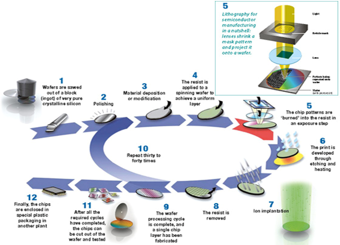
Lithography is perhaps your first time to hear this word but is not a fresh word in the semi-conductor industry. If you visit any semi-conductor fab today, you would see many lithography systems heavily be used in the manufacturing process where lithography plays a role to define tiny patterns to be printed on the wafer. The picture below shows the where the lithography is implemented in the semiconductor process cycle. Before a wafer is sent to the lithography system, several preprocessing are needed such as, polishing, deposition and resist coating. After litho exposure(step 5), the wafer will be etched and ion-implemented. Then this wafer can continue its second cycle to have the next layer built on top of it. These fabrication cycles will usually repeat at least 20 times depending on the chip applications.
Lithography system
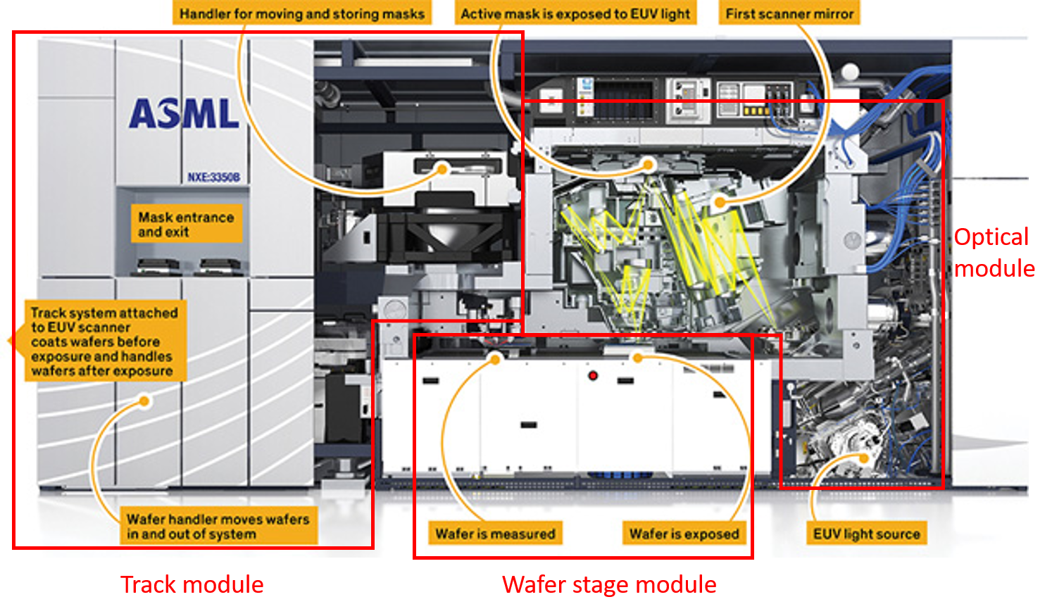
Since we know the lithography system plays an important role in chip fabrication process, why not just open this secret box to look how it works inside. The graph below on gives you an overview of how a frontier EUV system design looks like. This system can be generally broke down into three main modules which are already labeled in the graph, plus some additional assistant modules like cooling, power supply and air control… which are not indicated in this graph. For the track module you can interpreted it as a kind of IO interface towards the outside world. The reticles and the wafers will be loaded and unloaded via the track. This track system is usually interconnected with the fab pipeline in production. For the stage module, it manages the internal wafer flow. Before the wafer be placed under the projection box, the wafer topography must be measured and sent to the lithography system as the pre-alignment information. The final one is the optical module which governs the photon’s life from the beginning to the end. The detail of the opical module will be explained in the next session.
Lithography optics module
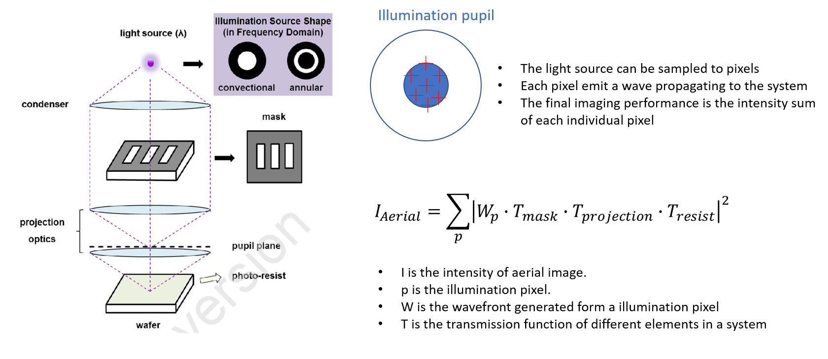
Lithography optics module consists of several sub modules, including source, illumination and projection. A simple way to understand the lithography optical module is to interpret it as a projector. Just imagine you need light to shine on the mask and this mask image needs to be demagnified and projected onto the wafer. The EUV light comes from the source vessel which generates EUV using laser and plasma. The mechanism of generating EUV source is out of scope of this post because we would like to concentrate on the scanner system. As the EUV light moves forward to the illumination module, the light will be modulated by the field facet mirrors which decides which pixel in the pupil plane will be switched on and which of them will be switched off. These pixels map to the illumination angles with which the EUV light shine on the reticle. The light will be diffracted by the reticle towards the projection optics module. As a result, the tiny grating patterns on the reticle will print on the wafer.
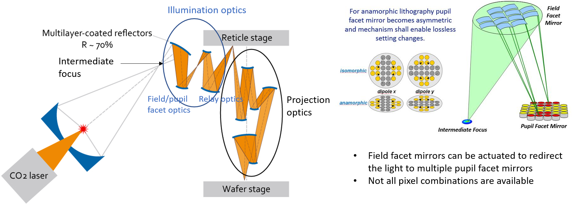
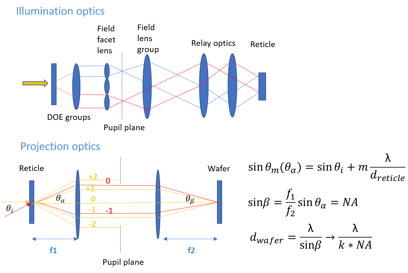
Mirror optics perhaps is not straightforward for most optical designers. Thereby, a lens-based optics module is shown in the next graph to explain some basis. In the lens-based illumination module, we see field facet lens array are included in the illumination design. The purpose of using field fact lens array is the same as using field facet mirror array, which is generating the pixel source point in the pupil plane. The DOE(Diffraction Optics Element) group prior to the field facet lens group functions as a modulator to control which facet lens would be illuminated. In short, the concept of the lens-based illumination module is entirely implemented in the EUV mirror-based illumination module. The limitation in EUV mirror optics is the freedom of the pixel choice. The relay optics provides additional knobs to fine tune the illumination performance on the reticle.
Projection optics is commonly seen ın an optical design. This design consist of an object plan, pupil plane and the image plane. Reticle would be placed at the object plan, and the light will be diffracted by the grating-type of patterns towards the projection system. In order to print these tiny features, at least the 0th order and the first order of the diffraction light must be captured by the projection pupil. As a result, the minimum printable pitch dwafer was predetermined by the pupil’s numeric aperture(NA) at wafer level(assuming the illumination angle is zero). However, the default minimum pitch is not small enough to cover today’s semiconductor feature size. We have to introduce off-axis illumination in the projection optics. This way we manipulate the diffraction angle of a gratting pattern such that at least 0th order and either +1 or -1 order can be captured by the projection pupil. This resolution enhancement technique(RET) is absorbed by the factor k of the formula in the graph. Knowing how to choose an optimum illumination pupil is a key to enable the pattern nodes in the lithography.
Lithography system performance modeling
As you have already seen in the pictures above, a lithography system is a complex giant box. You need a robust model to qualify and quantify the system performance. Although the system is working in the free space, we still need some finite element analysis when the light interact with the nano structure on the reticle. The entire modeling of a lithography system requires three simulators to complete imaging analysis when EUV light travels to mask, pupil and resist respectively.
Raytracing
Raytracing serves an integrated method to cascade the simulation results at different stages. When the light starts from the illumination source, it can be treated as an incoherent light source. The contribution of each individual pixel in the illuminated source could add up linearly in the final stage. As described in the formula below, each individual ray from the source has its mask transfer function, projection transfer function and the resist transfer function which modulate the wave amplitude and phase. With the contribution from each pixel, raytracing is a feasible approach to take care of the needs of each individual ray in the overall system modeling.
Mask Modeling
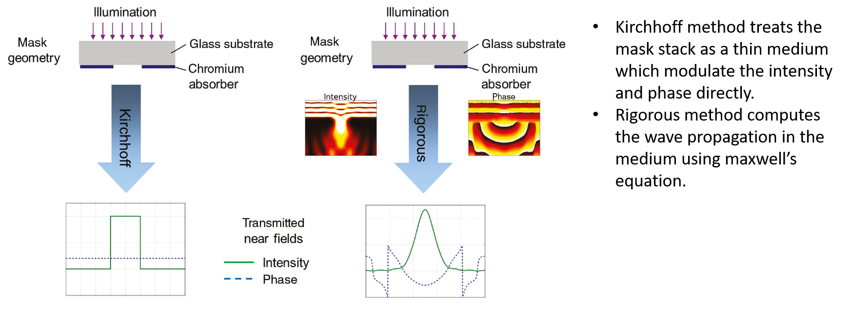
lithography mask is a multilayer film stack which allow certain bandwidth of light spectrum to transmit (or reflect from) the mask. On top of film stack there is a pattern layer which consists of a bunch of nano gratings such as dense line space, isolated line space and regular array. To understand the basic diffraction behaviour, a flat mask could be assumed, which is subjected to Kirchhoff’s diffraction formula to calculate the diffracted wave. The absorber within the pattern layer could modulate the light amplitude and phase, which determined the transmitted near-field from a mask. However, Kirchhoff’s formula is just an approximation of the real field. When the wavelength is at the same scale as the grating period, wave property is strongly dominant. Hence, a rigorous computation via maxwell equation is generally used to analyze the transmitted near filed from a mask. These rigorous methods are related to RCWA, FDTD and FEM approaches. Please see the figure below for the difference between Kirchhoff and rigorous method.
Projection and Aberrations
As briefly mentioned in the previous session, the easiest way to interpret a lithography system is to think it as a projector. The information on a mask needs to be projected onto a wafer, thereby a high contrast image is expected at the wafer level. We could use free space optics to analyze the image performance at the wafer level. Fourier optics is a good approcah to calcuate wave propagation from the transmitted near filed to the final image plane.
The resolution of image is limited by the diffraction limit in an ideal system. Shorter wavelength and larger numeric aperture are keys to reach smaller resolution. In addition to the diffraction limit, a real optical system also suffers from aberrations, intensity inhomogeneity and mechanical vibration. The first two system imperfections are modeled in the pupil plane as an intensity and phase modulation for the incoming propagated wave, where as the vibration is treated as the variety of tilt and focus in the system tolerance.
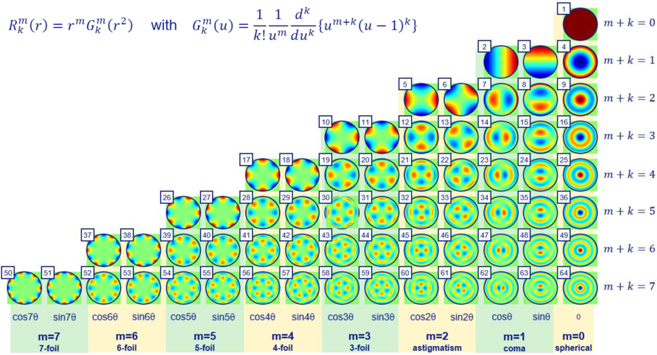
How to characterize aberrations properly is always an important question in the litho simulation. Unlike intensity inhomogeneity, aberration is less likely an arbitrary distribution in space, rather it is the outcome of the projection module design. As a result, litho engineers like to use Zernike polynomials to describe any aberration because they are orthogonal and are linked to the optical effect in projection. The table below shows the zernike polynomiasl up to Z64. They can be arranged in such an way that each columns could correspond to an aberration family that we are familar with in optics. For instance, spherical aberration will cause the image defocus, coma will cause the variety of magnification (center shift) over the entrance pupil, and astigmatism will cause different focus position for different patter orientation.
Resist chemistry
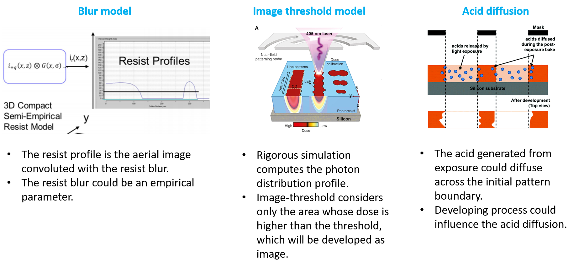
Resist is a photon-sensitive layer deposited on a wafer as a pattern-defined precursor for the subsequent etch process. The ADI (After-Litho-Image) quality is related to the aerial image quality and resist chemistry. When the photon comes into the resist, the photon will diffuse in the resist, causing the image to be blury. There are several models which are used to estimate the diffusion impact on imaging, such as blur model and image threshold model. The graph below gives more detail explanation for these two models.
Antoher aspect could be added into the resist modeling is to consider the chemical reaction in resist. Since PAG(photon-acid generator) convert photons to acid, the diffusion area of acid would decide the image boundary. If a different developing process is used, it will give a different impact to the final image.
Summary
Lithography is a real complicated ginant machine which took many years to be developed in industry. The litho process functions as an eye in the semiconductor manufacturing process. Without any pattern resolved in the resist, it is not possible to proceed with the subsequent steps. The imaging performance relies on a sophisticated and cascaded modeling which involves the knowledge in mask, projection and resist chemistry.