News
Advanced Semiconductor Packaging Market Forecast to Grow at 7.5% CAGR Through 2031
The Advanced Semiconductor Packaging Market is projected to grow from USD 18,090 million in 2024 to USD 29,800 million by 2031, at a CAGR of 7.5%. This growth is driven by the increasing demand for heterogeneous chiplet architectures and high-bandwidth memory stacks, particularly in telecommunications, automotive, and consumer electronics.
![]()
Launches
OKI Develops 124-Layer PCB Technology for Next-Generation AI Semiconductor Testing Equipment
OKI Circuit Technology has developed a 124-layer PCB for wafer inspection equipment, enhancing capabilities for high bandwidth memory used in AI semiconductors. This breakthrough aims to meet the growing demands of AI processing, improving data transfer speeds essential for AI applications.
![]()
Charts
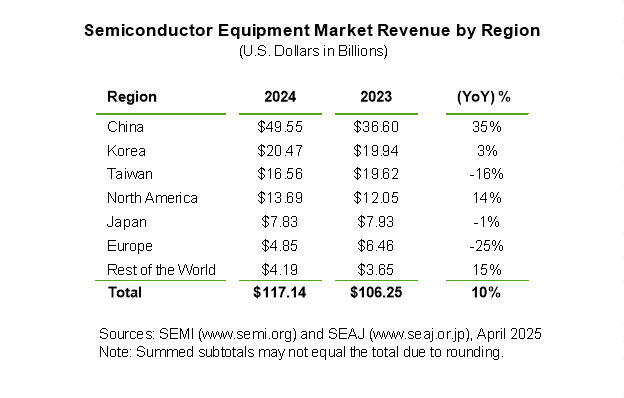
Global Semiconductor Equipment Sales Surge to $117 Billion in 2024
Sales of semiconductor manufacturing equipment rose 10% to $117.1 billion in 2024, driven by investments in advanced packaging and high-bandwidth memory technologies. This statistic underscores the industry’s response to the growing demand for AI and related applications.
Research
Investigating Charge Behavior in Multilayer OLEDs Using a Laser Spectroscopic Technique
Recent research from the University of California, Davis, utilized a novel laser spectroscopic technique to study charge behavior in multilayer OLEDs. This method allows for a better understanding of internal charge flow, which is crucial for improving OLED efficiency and performance in display technologies.

Insight
Q&A: Banned but Not Broken—How US Policy is Reshaping the Global Semiconductor Landscape
Valeria Bertacco, a semiconductor design expert, discusses how U.S. export restrictions are influencing the future of global semiconductor innovation. She predicts a shift in the market dynamics, emphasizing the need for U.S. companies to adapt to new realities while maintaining their competitive edge in chip design and manufacturing.
Stay tuned for more updates and analyses from the semiconductor industry as we navigate through these exciting times of innovation and development! For more insights and detailed articles, explore our website!