
News
This Machine Could Keep Moore’s Law on Track
ASML is pioneering high-numerical-aperture EUV lithography, aiming for commercial deployment in 2025. This advancement is crucial for maintaining Moore’s Law by enabling the production of increasingly smaller chip features, essential for next-generation devices.
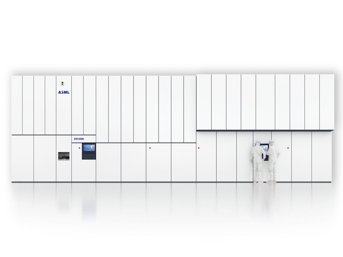
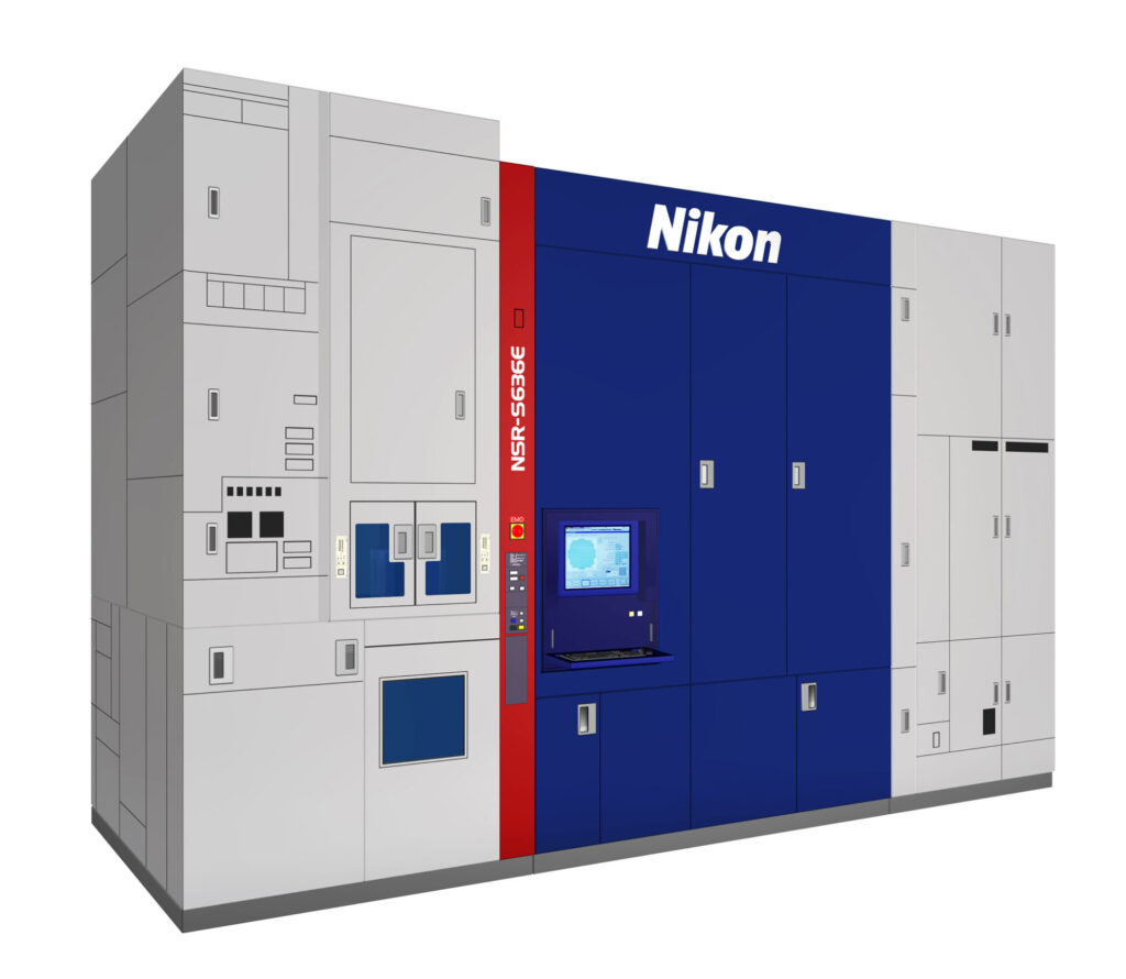
Launches
NSR-S636E ArF Immersion Scanner
Nikon introduces its NSR-S636E ArF immersion scanner, the most productive lithography system in its history, designed for critical layers in semiconductor manufacturing. This system enhances overlay accuracy and throughput, catering to the needs of advanced 3D semiconductor devices.
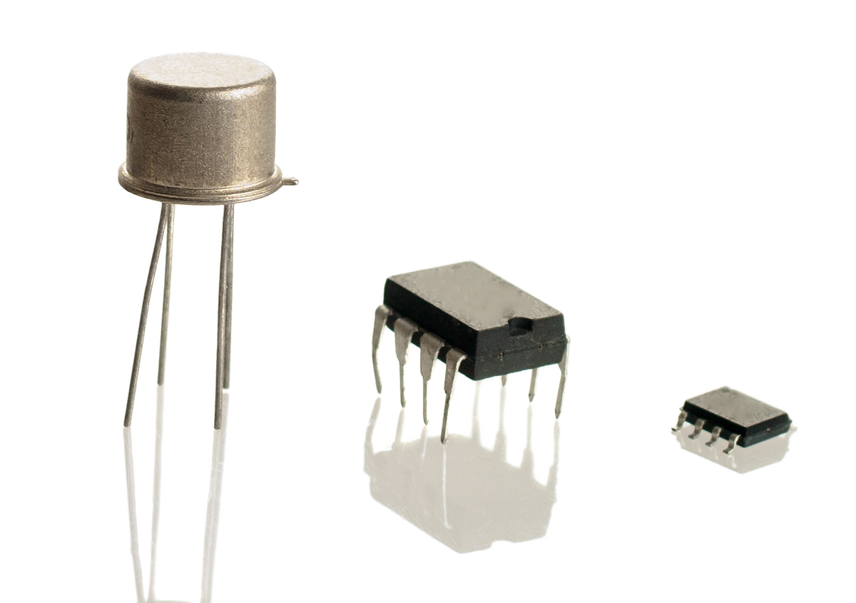
Charts
The State of the Transistor in 3 Charts
This article provides a comprehensive overview of the advancements in transistor technology over the past 75 years, emphasizing the exponential growth in transistor density and the ongoing miniaturization efforts critical for future semiconductor innovations.
Research
Scalable Approach For Fabricating Sub-10nm Nanogaps
Researchers have developed a progressive wafer-scale method for creating sub-10 nm nanogap structures, which promises significant advancements in semiconductor fabrication techniques, enhancing performance and scalability.

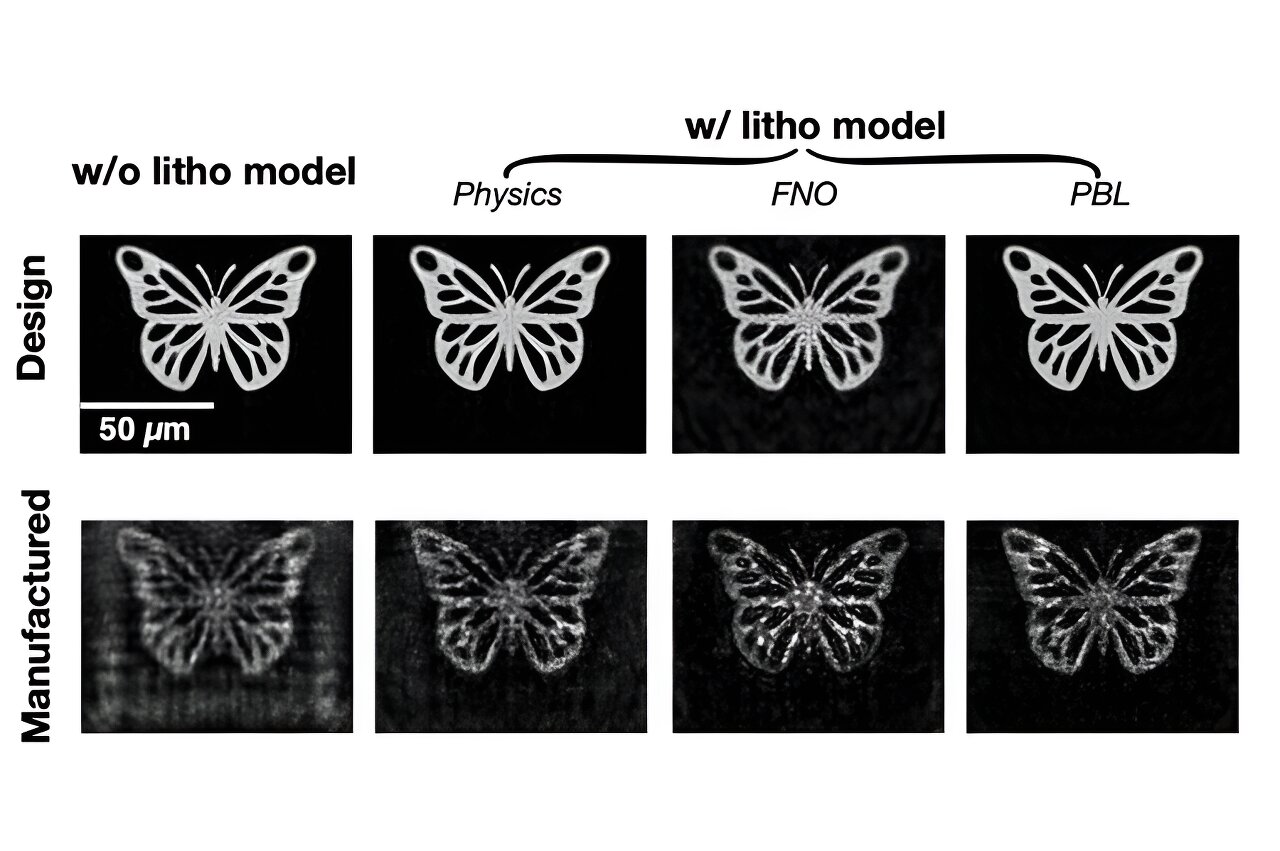
Insight
A New Method to Fabricate Optical Devices That More Closely Match Their Design Specifications
MIT and the Chinese University of Hong Kong researchers have developed a machine learning-based digital simulator for photolithography that significantly enhances the precision of optical device manufacturing, paving the way for improved performance in applications ranging from mobile cameras to telecommunications.
Stay tuned for more updates as we continue to bring you the latest news and innovations in the semiconductor industry!