
News
Other lithography approaches offer alternatives
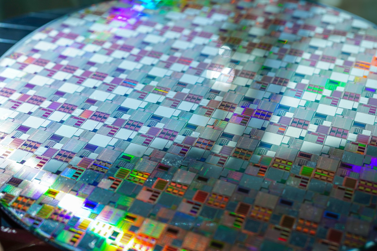
At the 2025 SPIE Advanced Lithography + Patterning conference, semiconductor manufacturers are exploring alternative lithography methods to enhance performance and reduce costs. Notable presentations included Micron Technology’s Tomohiro Iwaki discussing challenges in nanoimprint technology and Intel’s Florian Gstrein highlighting directed self-assembly techniques. These innovations aim to improve defect rates and boost yields, particularly relevant for logic and memory chips.

Launches
Getting PFAS out of lithography materials
Central Glass Co. is pioneering PFAS-free materials for 193-nm immersion lithography, addressing long-term environmental and health concerns associated with traditional photoresist components. Their new formulations, which include a PFAS-free photo acid generator and immersion barrier polymer, have shown promising results in maintaining performance while reducing harmful substances.

Charts
Chips – and lithography – head up and down
The latest insights from the 2025 SPIE conference emphasized the shift towards 3D semiconductor architectures to overcome scaling limitations. Presentations discussed how backside power delivery can alleviate power bottlenecks, enabling denser and more efficient chip designs. This transition is pivotal for sustaining Moore’s Law in an era of complex circuitry.

Research
Demonstration Of EUV Scatterometry On A 2D Periodic Interconnect
A research collaboration involving the University of Colorado, NIST, and Samsung has revealed advancements in EUV scatterometry, a metrology technique vital for measuring periodic nanostructured materials. The study demonstrates enhanced sensitivity and the potential for deep sub-nanometer precision, marking a significant step forward for semiconductor manufacturing.
Insight
Tokyo Electron Receives Renewal of DX-certified Business Operator Status from the Ministry of Economy, Trade and Industry
Tokyo Electron’s recent renewal of its DX-certified Business Operator status marks a significant achievement in its digital transformation initiatives. This renewed status emphasizes TEL’s commitment to leveraging digital technologies to enhance corporate value and adapt to the rapidly evolving semiconductor market, which is projected to approach $1 trillion by 2030.
Thank you for staying with us for the latest news in the semiconductor industry. We look forward to bringing you more updates on innovations and advancements in lithography and sustainability efforts.