
News
Hong Kong Kicked-off Construction of the First GaN Epi-Wafer Pilot Line
Hong Kong has launched its first ultra-high vacuum GaN epitaxial wafer pilot line, aiming to enhance its microelectronics industry. MassPhoton is set to invest HKD 200 million to develop GaN processes for optoelectronic and power devices, promising over 250 new jobs in the region.

Launches
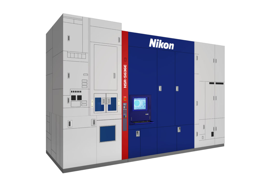
Nikon Announces Development of the NSR-S636E ArF Immersion Scanner
Nikon is developing the NSR-S636E ArF immersion scanner, designed for high-performance semiconductor manufacturing. This system promises superior overlay accuracy and ultra-high throughput, catering to the evolving demands of advanced semiconductor devices.
Charts
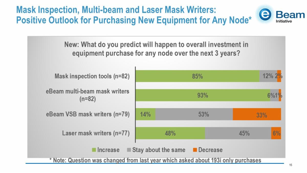
eBeam Initiative Survey Results Predict Strong Growth in Photomask Market
The eBeam Initiative’s latest survey shows that 100% of industry leaders expect an increase in mask revenues for 2024, highlighting the growing importance of photomasks in semiconductor manufacturing. Investments in multi-beam mask writers and inspection technologies are also anticipated to rise.
Research
New Protocol Improves Photolithography Accuracy
A new quantum lithography protocol enhances the accuracy of photolithography by addressing physical limitations. This advancement promises to improve the resolution of semiconductor devices, critical for meeting future manufacturing demands.

Insight
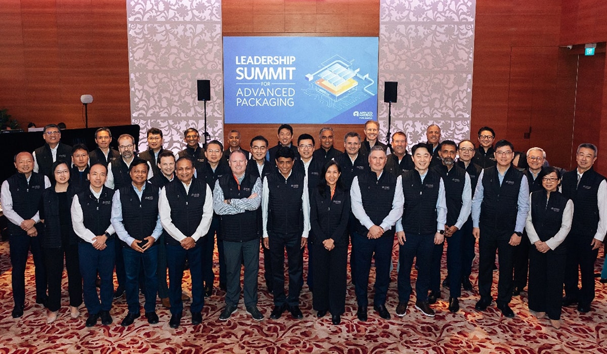
Semiconductor R&D Leaders Share Vision for Accelerating Advanced Packaging
Industry leaders discuss the challenges and opportunities in advanced packaging technology, emphasizing the need for tighter process control and the integration of heterogeneous technologies. Innovative strategies for attracting talent and improving curricula are also highlighted.
Stay tuned for more insights and developments in the semiconductor industry as we continue to bring you the latest news and trends.