
News
Intel: Back on Top by 2025?
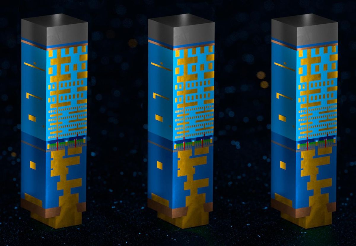
Intel has revealed an ambitious roadmap that aims to reclaim its leadership in semiconductor manufacturing by 2025. The company will discontinue the use of “nanometer” terminology, introducing new node names like Intel 7, Intel 4, and the groundbreaking Intel 20A, which will feature the innovative RibbonFET architecture for improved transistor performance and efficiency. The PowerVia technology will also enhance power delivery, promising significant advancements in the semiconductor landscape.
Launches
AI’s Impact: Three Examples
At the 2025 SPIE Advanced Lithography + Patterning conference, advancements in lithography systems and AI applications were showcased. ASML unveiled new lithography solutions that promise enhanced stability and measurement capabilities, while imec’s research on extreme ultraviolet lithography (EUVL) aims to improve chip yield through innovative assist features. These technologies are crucial for meeting the escalating demands driven by AI applications.

Charts
Photonics Aids the March of Moore’s Law
The importance of photonics in sustaining Moore’s Law is emphasized as TSMC aims for products with over one trillion transistors by 2030. The article discusses the evolution of technology nodes from 20 µm in 1968 to 2 nm today, highlighting how photonics advancements and chiplet technology are essential for achieving higher transistor densities while maintaining performance improvements.

Research
Research Allows for 3D Printing of ‘Organic Electronics’
Researchers at the University of Houston have developed a process for 3D printing organic semiconductor devices using multiphoton lithography. This technology enables the fabrication of flexible electronic circuits, biosensors, and bioelectronics with enhanced conductivity, paving the way for applications in biomedical fields and next-generation electronics.

Insight
CEO Interview with Jonas Sundqvist of AlixLabs
Jonas Sundqvist discusses the innovative Atomic Layer Etch (ALE) technology developed by AlixLabs, which aims to reduce costs and improve yields in semiconductor manufacturing. He highlights how their APS (ALE Pitch Splitting) process provides a sustainable alternative to traditional multi-patterning techniques, addressing key challenges in the semiconductor industry as it scales down feature sizes.

Stay tuned for more updates as we continue to explore the latest trends and innovations in the semiconductor industry!