
News
Tsinghua University Breaks Ground on EUV Photoresist in China’s Semiconductor Push
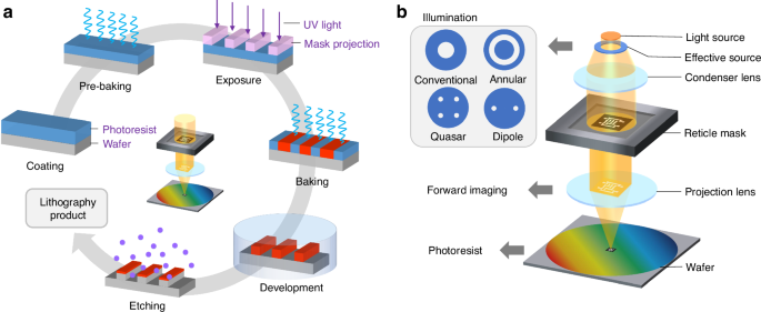
Tsinghua University has made significant strides in EUV lithography materials with a new polytellurium oxane-based photoresist. This advancement aims to enhance the efficiency of chip production at 7nm and below, critical for China’s semiconductor self-reliance strategy. The research indicates that the new photoresist effectively improves absorption efficiency and defect control, potentially revolutionizing the industry.

Launches
Researchers Identify Carbon Contamination as Key Barrier in Gallium Oxide Electronics
A team at Cornell University has pinpointed a carbon contamination issue that affects the performance of gallium oxide electronics. By using UV-ozone treatments, they have successfully reduced contact resistance, thus improving device reliability. This innovation paves the way for the commercialization of gallium oxide in high-power applications, including electric vehicles and grid infrastructure.

Charts
Global IC & Semi Market Report
TrendForce’s latest report provides an in-depth analysis of the semiconductor market’s size and growth trends, detailing the dynamics of memory, semiconductor components, and optoelectronic products. The report highlights market applications across various sectors, offering insights into competitive landscapes and regional market dynamics, essential for industry professionals strategizing for future developments.

Research
Advancements and Challenges in Inverse Lithography Technology: Review of AI-Based Approaches
This comprehensive review discusses the evolution of computational lithography, focusing on the integration of AI methods in inverse lithography technology (ILT). The paper outlines significant advancements, challenges, and future perspectives in using AI for enhancing lithography modeling accuracy and efficiency, a critical aspect for the semiconductor manufacturing process.
Insight
AI’s Role in Transforming Semiconductor Manufacturing
The ICT Applications Research department has released insights on the latest trends in semiconductor technology, including the impact of AI on the manufacturing process. This report provides valuable perspectives on how AI technologies are reshaping the semiconductor landscape, particularly in areas like predictive maintenance and process optimization, crucial for industry leaders adapting to rapid technological changes.
Stay with us for the latest news and insights in the semiconductor industry as we continue to monitor advancements and trends that shape our future.