
News
SEALSQ Announces Deal With Quantix Edge Security to Develop Spain’s First Post-Quantum Semiconductor Personalization Center
SEALSQ Corp has signed a definitive agreement with Quantix Edge Security to create Spain’s first post-quantum semiconductor personalization center in Murcia. This project aligns with the Spanish government’s strategy to strengthen sovereignty in critical sectors like semiconductors and cybersecurity, projected to generate significant economic impact and support the commercialization of quantum-resistant technologies.

Launches
Packaged Optics for AI Datacenter Scale
Alchip Technologies and Ayar Labs have unveiled a co-packaged optics solution that addresses data movement bottlenecks in AI infrastructure. This innovation aims to enhance network connectivity and efficiency, crucial for scaling large AI clusters, by replacing traditional copper interconnects with optical solutions.
![]()
Charts
ECTC Hears Call for Power Optimization
At ECTC 2025, AMD’s Sam Naffziger emphasized the unsustainable rise in power demands due to AI. A chart presented highlights the exponential growth in compute demands driven by AI applications, displaying the urgent need for innovations in power efficiency through 3D packaging and hybrid bonding technologies.

Research
Atomic Neighborhoods in Semiconductors Provide New Avenue for Designing Microelectronics
A groundbreaking study reveals that semiconductors exhibit distinct short-range order (SRO) patterns that can alter their electronic properties. This research opens new pathways for tailoring semiconductors for quantum computing and optoelectronic applications, providing insights into atomic arrangements that influence functionality.

Insight
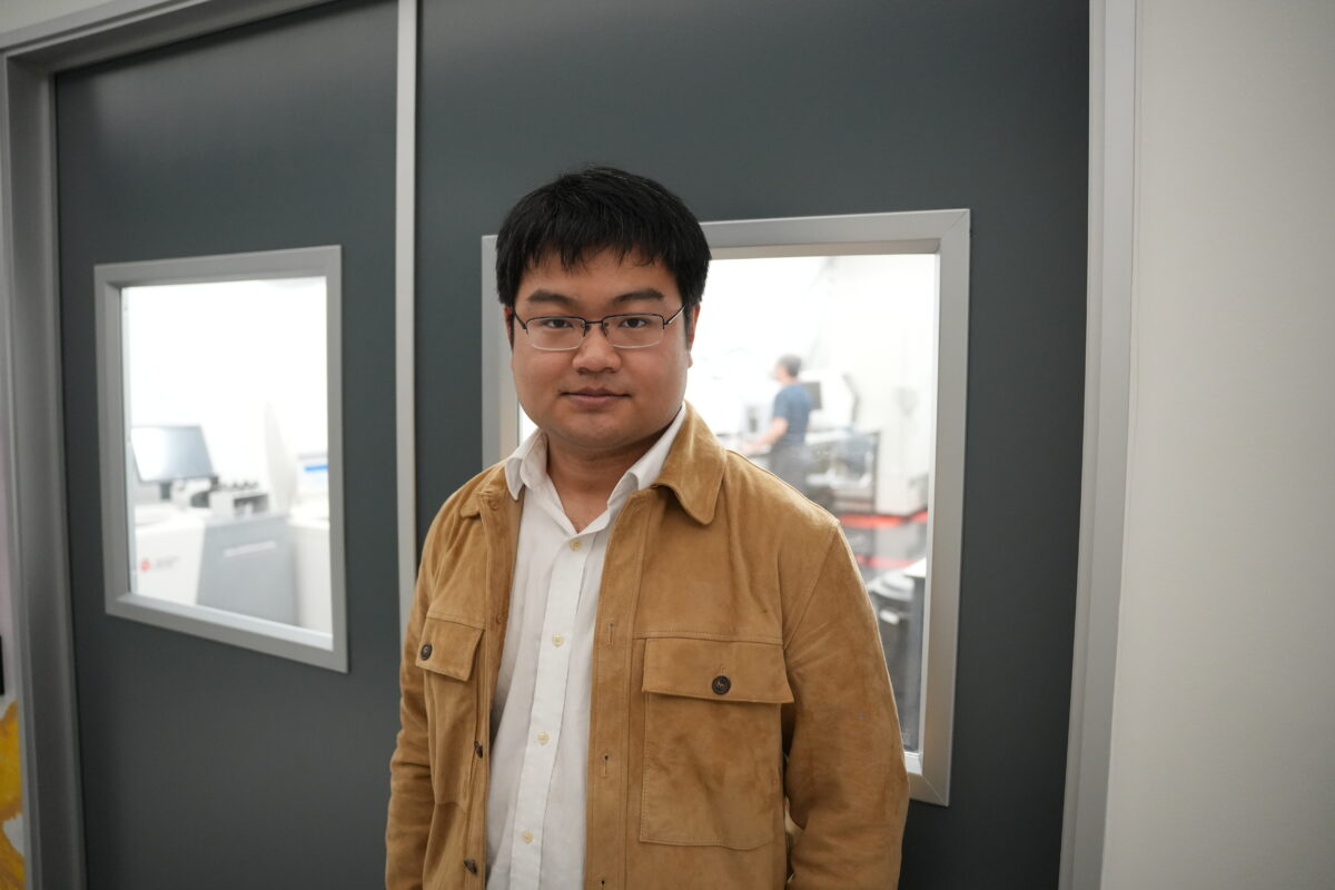
CEO Interview with Jiadi Zhu of CDimension
Jiadi Zhu discusses CDimension’s focus on 2D semiconductor materials that significantly improve power efficiency and noise reduction in chips. He emphasizes the shift from silicon to innovative materials as vital for addressing the industry’s increasing power demands and enabling breakthroughs in quantum computing.
Stay updated with our newsletter for the latest advancements and insights in the semiconductor industry.