
News
ASML, Mistral AI enter strategic partnership
ASML has announced a strategic partnership with Mistral AI, which involves a significant investment of 1.3 billion EUR. This collaboration aims to enhance ASML’s product offerings through AI integration, focusing on improving lithography systems for faster and more efficient semiconductor manufacturing.
Launches
NSR-S333F ArF Scanner Now Open for Orders
Nikon has launched its latest ArF scanner, the NSR-S333F, designed for high overlay accuracy and productivity. This scanner, built on advanced technology, is set to meet the growing demand for precision in semiconductor manufacturing.

Charts
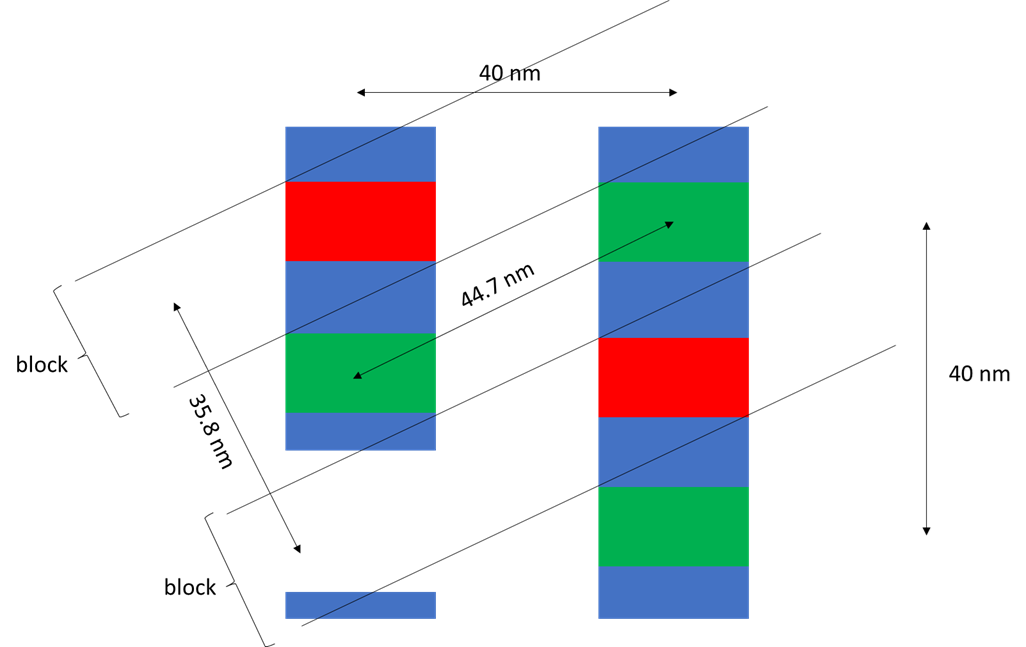
Via Multipatterning Regardless of Wavelength
A detailed analysis highlights that the minimum metal pitch for the 2nm node could reach 20 nm or less, necessitating advanced multipatterning techniques. This chart underscores the increasing complexity and need for innovation in semiconductor patterning as technology advances.
Research
First Stage Of Nanoscale Imaging In Positive-Tone EUV Photoresists
Researchers from Berkeley Lab have published insights into how the polymer sequence in positive-tone EUV photoresists affects imaging processes. Their findings could refine the understanding of resist performance and lead to improved resolution in semiconductor manufacturing.

Insight
PLDC: A Robust MPC Solution for Any Mask Shape
At SPIE Photomask Japan 2025, Micron discussed their new pixel-level dose correction technology, PLDC, which enhances efficiency in mask shops. This development signals a significant leap towards optimizing mask production processes for advanced semiconductor fabrication.

Stay tuned for more updates as we continue to cover the latest innovations and developments in the semiconductor industry!