
News
Double Duty Logic Block Architecture Enabling Concurrent LUT and Adder Chain Usage
A new technical paper from researchers at Nanyang Technological University and other institutions presents the “Double Duty” FPGA architecture, which allows for concurrent use of LUTs and adder chains. This innovation enhances arithmetic density in FPGAs, achieving significant area reductions without affecting critical path delay. The proposed architecture promises a 9.7% improvement in area-delay product, making it a significant advancement for FPGA applications.

Launches
The path to smaller denser and faster
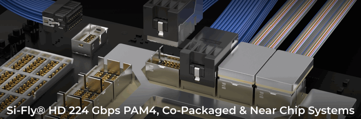
Samtec is set to host a webinar discussing its new co-packaged copper (CPC) and co-packaged optics (CPO) solutions, termed CPX, which enable advanced speeds of 224 Gbps. This integration aims to enhance performance in data centers and AI systems, addressing the common narrative that “copper is dead.” The event will showcase how combining copper and optical technologies can optimize interconnect strategies.
Charts
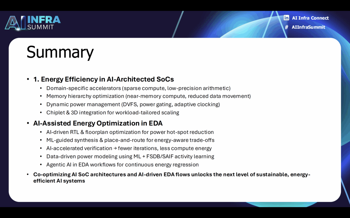
AI Everywhere in the Chip Lifecycle: Synopsys at AI Infra Summit
Synopsys showcased an AI-driven ecosystem that integrates energy efficiency and accelerated design processes at the AI Infra Summit 2025. Key charts from the presentation illustrated how AI is now an end-to-end engine driving chip development, with the potential to reduce design times by up to 40% and improve energy efficiency amidst soaring AI workloads.
Research
In-SRAM Computing Architecture Tailored For Cryptographic Acceleration Within MCUs
Researchers from UC Riverside have introduced CryptoSRAM, an innovative in-SRAM computing architecture that enhances cryptographic operations directly within microcontroller units (MCUs). This architecture reportedly achieves throughput improvements of up to 74× for AES encryption compared to traditional software implementations, addressing performance and energy costs in IoT devices.

Insight
CEO Interview with Howard Pakosh of TekStart
In this insightful interview, Howard Pakosh discusses how TekStart has transitioned into a venture builder focused on semiconductors and AI. He highlights the innovative solutions being developed, particularly through their ChipStart business unit, which addresses critical industry challenges like energy efficiency and supply chain fragility, particularly in Edge AI applications.

Stay tuned for more updates as we continue to bring you the latest innovations and trends in the semiconductor industry!