
News
Group including Nvidia, BlackRock buying Aligned Data Centers in deal worth about $40 billion
A consortium featuring BlackRock, Nvidia, and Microsoft is set to acquire Aligned Data Centers in a substantial $40 billion deal. This strategic investment aims to bolster and expand critical next-generation cloud and artificial intelligence (AI) infrastructure. The acquisition addresses the burgeoning demand for robust computing resources and data center capacity fueled by the rapid growth of the AI sector. Aligned Data Centers brings a formidable portfolio of 50 campuses and over 5 gigawatts of operational and planned capacity across the U.S. and Latin America. As the inaugural transaction for the Artificial Intelligence Infrastructure Partnership (AIP), this initiative plans to mobilize $30 billion in initial equity capital, with potential to scale to $100 billion including debt, highlighting the immense capital flowing into AI infrastructure development.

Launches
Athos Spins Out Of Mercedes With Chiplet Concept for AVs
Athos Silicon has officially spun out of Mercedes-Benz, emerging from a five-year research project focused on creating functionally safe compute solutions for autonomous vehicles (AVs). Mercedes-Benz has provided a strategic investment, including substantial intellectual property, and will continue to collaborate on Athos’s mSoC reference design, Polaris. The Polaris architecture is designed with functional safety as a primary consideration, leveraging a chiplet-based approach that integrates three compute dies, a central cache, and an NPU, all sourced from third-party suppliers. A core innovation is Athos’s unique voting mechanism, which uses an odd number of chiplets (starting with three) to ensure continuous safety by monitoring for both software and hardware issues. This design promises enhanced performance and reliability at a lower cost, extending its applications beyond automotive to other autonomous systems like drones and robots.

Charts
Microelectronics and Advanced Packaging Technologies Roadmap 2.0 (SRC)
The Semiconductor Research Corporation (SRC) has unveiled its comprehensive Microelectronics and Advanced Packaging Technologies (MAPT) Roadmap 2.0. This updated industry-wide framework, which represents the first 3D semiconductor roadmap, incorporates contributions from over 370 experts across 132 organizations. Funded by the U.S. Department of Commerce’s NIST and developed to support the CHIPS Act, the roadmap provides a crucial strategic guide for the entire semiconductor supply chain. Notably, it includes a new chapter dedicated to digital twins and their applications, reflecting the evolving landscape of semiconductor design and manufacturing. The MAPT Roadmap 2.0 is an essential resource for guiding R&D, investment, and collaborative efforts within the global semiconductor ecosystem.

Research
CMOS 2.0 is Advancing Semiconductor Scaling
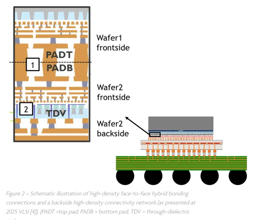
Imec’s recent breakthroughs in wafer-to-wafer hybrid bonding and backside connectivity are pioneering the development of “CMOS 2.0,” a significant paradigm shift in chip design. CMOS 2.0 addresses the traditional limitations of CMOS scaling by segmenting System-on-Chip (SoC) designs into specialized functional tiers. Each tier is meticulously optimized for specific requirements, such as high-performance logic, dense memory, or superior power efficiency, through advanced system-technology co-optimization (STCO). This innovative approach leverages 3D interconnects and backside power delivery networks (BSPDNs) to enable ultra-dense connections and power distribution on both sides of the wafer. At VLSI 2025, Imec showcased impressive advancements, including 250nm pitch wafer-to-wafer hybrid bonding and 120nm pitch through-dielectric vias (TDVs). These technologies facilitate sophisticated heterogeneous stacking and enhance power efficiency by drastically reducing IR drops and decongesting frontside interconnects, which is critical for future mobile SoCs and AI accelerators.
Insight
The Rise, Fall, and Rebirth of In-Circuit Emulation
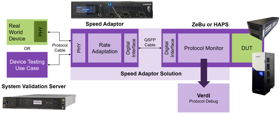
This in-depth article, featuring insights from Synopsys’s distinguished experts, chronicles the remarkable resurgence of in-circuit emulation (ICE) in system-level validation, largely driven by the evolution of third-generation speed adapters. Defying previous predictions of its obsolescence, modern ICE platforms, particularly those integrating Synopsys Speed Adapters and the System Validation Server (SVS), are proving indispensable for critical pre-silicon bug detection. Through compelling real-world case studies, the article demonstrates how high-fidelity ICE environments can uncover elusive RTL flaws, timing mismatches, and complex interoperability issues tied to low-level system behavior and physical layers (e.g., PCIe Gen5, UFS, Ethernet, MIPI sensors) that often escape virtual verification methods. By accurately simulating real-world operating conditions and rigorously enforcing design specifications, ICE significantly mitigates the risk of costly re-spins and accelerates time-to-tapeout, solidifying its role as an essential tool in the development of today’s increasingly complex semiconductor designs.
Stay connected for the latest innovations and breakthroughs shaping the future of the semiconductor industry!