
News
ASML and Mistral AI Forge Strategic Partnership to Advance Lithography with AI
ASML Holding NV has announced a strategic partnership with France-based AI leader Mistral AI, backed by a significant €1.3 billion investment in Mistral AI’s Series C funding round, resulting in ASML holding an approximately 11% share. This long-term collaboration aims to integrate advanced AI models across ASML’s entire product portfolio, including research, development, and operations. The partnership seeks to:
- Deliver innovative products and solutions to ASML customers.
- Accelerate time to market and enhance the performance of holistic lithography systems.
- Explore potential for joint research to address future opportunities in the semiconductor and AI value chain.
As part of the investment, ASML Chief Financial Officer Roger Dassen will join Mistral AI’s Strategic Committee, providing an advisory role in the AI company’s future strategy and technology decisions.
Launches
3D Printable Photochromic Materials Enable All-Optical Processors
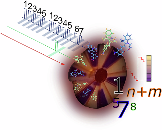
Researchers have developed novel 3D-printable photochromic materials that enable all-optical processors capable of performing arithmetic operations using light. These materials, based on an oligomer and photoinitiator doped with photochromic molecules (SP or BTF6), dynamically switch between colorless and colored states upon exposure to UV and green light.
- Key Functionality: The photochromic properties allow for dynamic control of light signals, enabling multi-step photoswitching.
- Arithmetic Operations: Demonstrated arithmetic operations like addition and division, and logic gates (NOT, NOR), by precisely controlling light transmission through the material.
- Architectural Innovation: The technology supports new architectures, including 3D spiral-shaped components for parallel processing, where each element can be individually addressed.
- Enhanced Stability: BTF6-doped samples exhibit exceptional thermal stability, retaining their encoded configurations for over twelve months, making them highly suitable for long-term data storage applications.
Charts
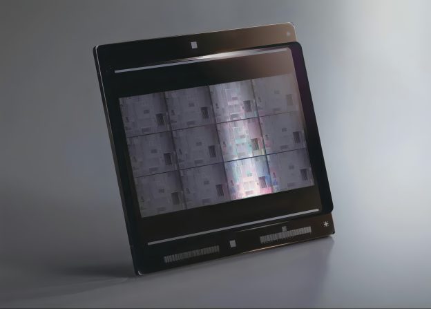
Samsung Ventures into Photomask Outsourcing While Eyeing New EUV Mask Technologies
Samsung is reportedly initiating its first-time outsourcing of lower-end photomasks, specifically i-line and KrF masks for memory chip production, to external suppliers such as PKL and potentially Tekscend Photomask. This strategic shift is driven by several factors:
- Resource Reallocation: Allows Samsung to dedicate internal resources and R&D efforts towards advanced ArF and EUV photomask production for cutting-edge logic chips.
- Market Dynamics: The South Korean photomask market, valued around the mid-700 billion won range last year, is experiencing high demand with domestic manufacturers operating above 90% capacity, indicating potential supply chain impacts for rival foundries.
- Technological Push: Samsung is accelerating the adoption of Phase Shift Masks (PSM) in logic semiconductor manufacturing, developing methods to apply PSM to EUV lithography processes to achieve enhanced precision for sub-3nm patterning.
- Increasing Demand: The number of photomasks required for advanced DRAMs has surged from 30-40 to over 60, primarily due to the increasing complexity of multi-patterning techniques.
Research
Unraveling Nanoscale Imaging in Positive-Tone EUV Photoresists
A new technical paper by researchers at Lawrence Berkeley National Laboratory and Columbia Hill Technical Consulting investigates the initial stages of nanoscale imaging in positive-tone Extreme Ultraviolet (EUV) photoresists. The study focuses on understanding how polymer chain structure influences the radiolytic process that defines image resolution.
- Process Overview: EUV exposure in photoresists is a radiolytic process that generates electrons, radicals, and ions, which are critical for defining the printed image.
- Research Focus: The study simulated the sub-picosecond stages of imaging, specifically evaluating the influence of defined sequence and random copolymer structures on radiolytic spur formation—clusters of species formed by electron-polymer interactions.
- Key Finding: Computational results, validated against literature on electron thermalization, revealed that the polymer sequence has no significant effect on spur composition. This implies that potential imaging improvements from polymer sequence control would likely arise from subsequent lithographic process steps rather than the initial EUV exposure itself.

Insight
Understanding How Secondary Electrons Worsen EUV Stochastics and Limit Dose Returns
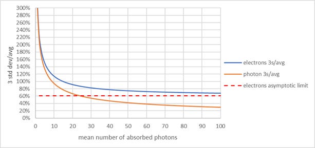
In EUV lithography, increasing dose leads to diminishing returns in reducing stochastic effects, as electron noise increasingly dominates over photon noise. A recent analysis highlights the direct contribution of electrons to these stochastic variations:
- Electron Variability: Each absorbed EUV photon releases a random number of photoelectrons and subsequent secondary electrons, creating significant statistical fluctuations in energy deposition.
- Dose Limitations: Unlike classical photon shot noise, which decreases with increasing dose, electron noise exhibits an asymptotic limit. This means that at higher doses, electron noise becomes the dominant factor, severely limiting further improvements in stochastic behavior.
- Blurring and Defects: Electron scattering causes a blurring effect that reduces image contrast. Local fluctuations in electron density are more likely to cross printing thresholds, potentially leading to critical defects such as microbridging, especially along feature edges.
- Scaling Challenges: As feature sizes shrink to 10 nm half-pitch and below, pixel sizes decrease, resulting in fewer absorbed photons per pixel even with increased dose. This exacerbates both photon and electron noise, leading to higher probabilities of defect formation.
Stay tuned for more cutting-edge developments and insights shaping the semiconductor landscape!