News
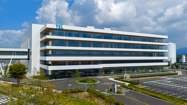
Tokyo Electron Completes Construction of New Development Building in Kyushu
Tokyo Electron (TEL) has announced the completion of its new Process Development Building in Koshi-shi, Kumamoto, for its manufacturing and development subsidiary, Tokyo Electron Kyushu. This 47 billion yen investment underscores TEL’s commitment to innovation in semiconductor manufacturing equipment, including:
- Next-Generation Development Hub: The new facility will focus on developing coater/developers, cleaning systems, and advanced 3D packaging equipment like wafer bonders.
- Driving Innovation: These products are crucial for enabling ultra-high speeds, large capacities, high reliability, and power efficiency in semiconductor devices, supporting trends in finer scaling and higher integration.
- Sustainable Growth: The building is designed for advanced, efficient operations leveraging digital technologies, prioritizing safety, quality, and environmental considerations to deliver high-value products to customers.
Launches
Lam CVP David Fried Shares with EE Times How Fabtex™ Yield Optimizer Is Transforming Semiconductor Manufacturing with Virtual Twins and AI
Lam Research has introduced Fabtex™ Yield Optimizer, a new tool under its Semiverse® Solutions platform, aimed at tackling yield variability in high-volume semiconductor manufacturing. This innovative solution leverages advanced computational techniques to:
- Reduce Process Variability: Combines virtual silicon digital twins with inline fab data and optimization algorithms.
- Accelerate Issue Resolution: Helps manufacturers quickly identify and fix defects, leading to faster cycle times and reduced wafer waste.
- Cost Savings: Significant operational benefits for fabs by making virtual silicon more representative of real-world fab variations and targeting systematic yield-limiting mechanisms simultaneously.
Charts
SEMI Reports Record Semiconductor Equipment Sales in 2023, Forecasts Growth
The global semiconductor equipment market continues its robust growth trajectory, driven by increasing demand for advanced chips. According to SEMI, equipment sales are expected to rebound strongly, indicating sustained investment in manufacturing capacity and technology upgrades.
- Market Resilience: Despite recent fluctuations, the semiconductor equipment market demonstrated strong performance, with record sales indicating healthy industry fundamentals.
- Regional Investment: Specific regions show significant investment, reflecting strategic moves in manufacturing and supply chain localization.
- Future Outlook: Industry forecasts predict continued growth, driven by expansion in AI, HPC, and IoT sectors, necessitating advanced fab equipment.

Research
NextSilicon Details Runtime Reconfigurable Architecture
HPC silicon startup NextSilicon has unveiled its innovative runtime-reconfigurable hardware architecture, demonstrating potential to outperform traditional CPUs and GPUs for scientific computing and HPC benchmarks. Key aspects of their Maverick2 chip include:
- Runtime Reconfigurability: The dataflow chip dynamically reconfigures its hardware during runtime to accelerate “hot paths” (1% of code running 99% of the time), mitigating code bottlenecks in nanoseconds.
- Dataflow Processing: Unlike traditional architectures, NextSilicon’s chip dedicates most silicon area to compute blocks (ALUs), optimized for computation-heavy workloads and avoiding memory bottlenecks.
- Software Compatibility: The architecture supports any existing code (C++, Fortran, Python, CUDA, AI frameworks) without requiring rewrites, compiling it for both host CPU and reconfigurable hardware.
- Impressive Benchmarks: Test results on TSMC 5nm Maverick2 silicon show significant performance gains in Stream (5.2 TB/s), GUPS (32.6 GUPS at 460W), HPCG (600 GFLOPS at 600W), and PageRank (10x better than GPUs at half the power).
- Future Vision: NextSilicon is also developing a 10-wide RISC-V CPU, Arbel, as a host for its next-gen accelerator, Maverick3, aiming for vertical integration and enhanced performance.

Insight
Silicon Valley Events Highlight Innovation from Power to Edge AI
Recent Silicon Valley events, including OCP Summit, Synaptics Tech Day, and Infineon’s OktoberTech, showcased a rapid pace of innovation driven by the explosive growth of AI. Industry leaders emphasized key trends and challenges:
- AI Power Demands: A predominant concern is the massive power consumption of AI data centers, spurring innovation in cooling methods, 800V DC power solutions, and advanced packaging for efficiency.
- Ecosystem Collaboration: The necessity for industry-wide collaboration and open standards was a recurring theme, with a realization that no single company can tackle the immense challenges, such as co-packaged optics, alone.
- Edge AI Evolution: Discussions at Synaptics Tech Day highlighted the maturation of edge AI, moving beyond fragmentation towards “intelligence of things” through open edge AI initiatives and partnerships with major tech players.
- Quantum Computing on the Horizon: Infineon’s event underscored the growing relevance of quantum computing, with leaders asserting that it is “already happening now” and engineers should not be complacent.
- Silicon Valley’s Resurgence: Attendees noted an unprecedented energy and collaborative spirit in Silicon Valley, indicating a thriving environment for invention and problem-solving across hardware and software.

Stay connected with us for the latest news and in-depth analysis shaping the future of the semiconductor industry.