
News
Automotive Chiplet Forum 2025 Drives Collaboration for Next-Gen Vehicles
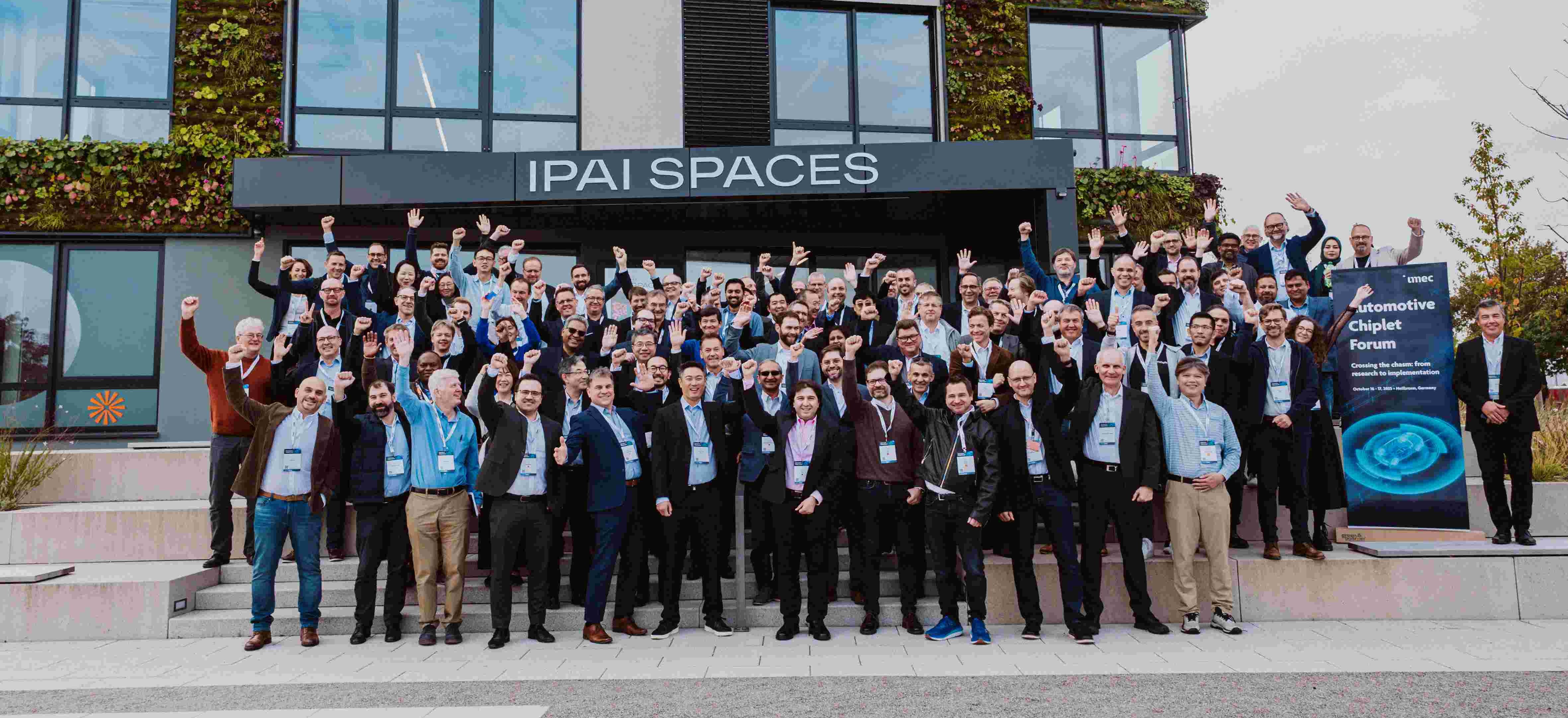
The fall 2025 Automotive Chiplet Forum (ACF) in Heilbronn, Germany, highlighted a significant expansion of imec’s Automotive Chiplet Program (ACP). Key developments include:
- GlobalFoundries (GF) joined as a foundry partner, bringing advanced manufacturing capabilities and a global footprint.
- Infineon, Silicon Box, STATS ChipPAC, and TIER IV (leader in autonomous driving) committed to participate, strengthening the ecosystem.
- Discussions centered on the vision of building the “Airbus” of automotive high-performance computing (HPC) through chiplet-based platforms, reinforcing Europe’s leadership.
- The event coincided with the inauguration of imec’s new Baden-Württemberg office, dedicated to automotive chiplet innovation.
The forum emphasized that achieving digital sovereignty in automotive compute requires industry and government alignment on interoperable chiplets built on open standards.
Launches
NextSilicon Unveils Runtime-Reconfigurable Architecture for HPC
NextSilicon, an HPC silicon startup, has detailed its runtime-reconfigurable hardware architecture and showcased impressive benchmark results for its Maverick2 chip, built on TSMC 5nm.
- The Maverick2 dataflow chip is designed to replace traditional CPUs and GPUs in supercomputers by reconfiguring during runtime to accelerate code bottlenecks.
- Its smart software algorithm continuously monitors applications, identifies critical “hot paths,” and reconfigures the chip in nanoseconds.
- The architecture leverages dataflow processing, dedicating most silicon area to compute blocks (ALUs), enabling more computation per clock cycle.
- NextSilicon’s stack can run any existing code (C++, Fortran, Python, CUDA, etc.) out of the box, offering flexibility for AI models and novel mathematical operations.
- Benchmarks show superior performance: 5.2 TB/s bandwidth in Stream, 32.6 GUPS at 460W, 600 GFLOPS at 600W for HPCG (outperforming CPUs/GPUs), and 40 gigapages/s for PageRank (10x better than GPUs).
- The company also unveiled test silicon for Arbel, a 10-wide RISC-V CPU aimed at enterprise-grade performance, comparable to Intel’s Lion Cove or AMD Zen 5.

Charts
Chiplets Poised for Explosive Growth, Fueling Next-Gen AI Systems
Chiplets are rapidly becoming the cornerstone of advanced AI systems, projected to reach a substantial market value by 2035.
- The multi-die designs, which break down large SoC functions into smaller, reusable dies, are forecasted to become a $411 billion market by 2035.
- This growth is driven by the fact that traditional SoC scaling can no longer meet the demanding compute and I/O needs of modern AI workloads, making modular chiplets a crucial solution.
- Interconnect performance, with UCIe (Universal Chiplet Interconnect Express) emerging as the preferred die-to-die standard, is critical for chiplet success.
- Advanced packaging techniques, including 2.5D and 3D approaches, are central to integrating these chiplets, requiring early co-design to manage thermal, mechanical, and power integrity challenges.
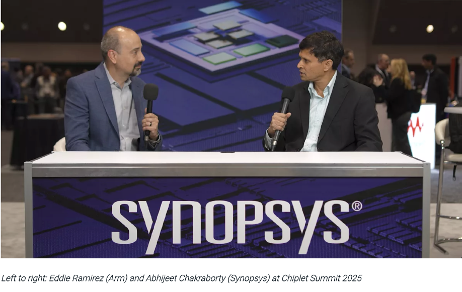
- Collaborations, such as that between Synopsys and Arm, are essential to streamline AI chip design, focusing on interoperability, reliability, and security within the evolving chiplet ecosystem.
Research
Stanford Researchers Pioneer Low-Temperature Diamond for Advanced Chip Cooling
Groundbreaking research from Stanford University has unveiled a method to grow polycrystalline diamond at low temperatures, offering a revolutionary solution for chip cooling.
- As transistors miniaturize and power densities soar, heat management becomes critical, with hot spots causing performance throttling and device degradation.
- Diamond, a highly thermally conductive yet electrically insulating material, has been challenging to integrate due to high growth temperatures (over 1,000 °C).
- Researchers achieved low-temperature growth (below 400 °C) by adding oxygen, which selectively etched away non-diamond carbon deposits, allowing large-grained polycrystalline diamond to form around devices.
- A key discovery was the formation of a silicon carbide interlayer at the diamond-semiconductor boundary, acting as a “bridge” for phonons and significantly reducing thermal boundary resistance.
- Initial tests on gallium-nitride (GaN) high-electron-mobility transistors (HEMTs) showed channel temperatures dropped by a remarkable 70 °C, boosting RF signal amplification fivefold.
- This innovation holds immense potential for high-power CMOS chips and 3D-stacked architectures, where “thermal scaffolding” with diamond layers and pillars could extract heat efficiently from multiple layers.

Insight
AI Transforms IC Manufacturing While ICs Fuel AI: Key Takeaways from SEMICON West
SEMICON West 2025 highlighted a virtuous cycle where AI is reshaping semiconductor manufacturing and design, while advanced ICs power the AI revolution. Industry leaders discussed the massive opportunities and challenges.
- AI Factories & Physical AI: Nvidia’s Timothy Costa emphasized $2 trillion opportunities in AI factories and physical AI, requiring innovation across semiconductor design, manufacturing, and AI. This includes accelerated design workloads, agentic AI for engineers, digital twins for fabs, and vision AI for defect detection.
- Digital Twins for Yield Optimization: Joseph Ervin of Lam Research showcased how fab-centric digital twins, leveraging virtual process modeling and machine learning, are crucial for rapidly boosting yield and shortening yield ramps in high-volume manufacturing, especially as process windows shrink.
- Sustainability & Energy Efficiency: Executives from ASM, IBM Research, Merck KGaA, and TEL America stressed the urgent need to combine technology development with sustainability, addressing the immense power consumption of AI data centers. Materials innovation and integrated development processes are key to energy-efficient scaling.
- Democratizing Design with AI: Mukesh Khare from IBM Research highlighted the role of agentic AI and open ecosystems in democratizing chip design, aiming for a 50% improvement in productivity for complex chip design activities.
- Continuous Innovation: The discussions underscored a newfound drive to accelerate the development of materials, equipment, processes, and servers, while simultaneously improving operating efficiencies across the entire supply chain.

Stay tuned for more cutting-edge developments and expert analysis shaping the semiconductor landscape!