
News
Chiplets: Powering the Next Generation of AI Systems
The semiconductor industry is rapidly shifting towards modular multi-die designs, with chiplets projected to become a $411 billion market by 2035. This paradigm allows for dividing large SoC functions into smaller, reusable dies, integrated into a single system-in-package (SiP) to overcome traditional SoC scaling limits. Critical to this evolution are interconnect standards like UCIe and advanced packaging techniques (2.5D and 3D). Collaboration between industry leaders like Synopsys and Arm is crucial, simplifying AI chip design by focusing on interoperability, reliability, and security within evolving chiplet ecosystems.
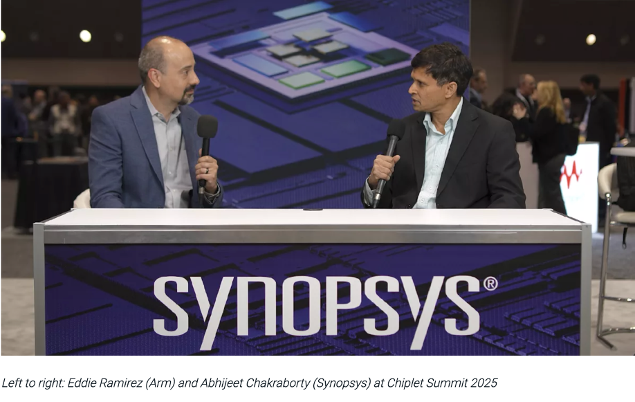
- Chiplets are set to be a $411 billion market by 2035, driven by AI’s compute and I/O demands.
- UCIe is emerging as the preferred die-to-die interconnect standard, alongside advanced packaging techniques.
- Industry collaboration, such as between Synopsys and Arm, is vital for streamlining AI chip design and ensuring interoperability.
Launches
VSORA: Inference Acceleration from the Ground Up
VSORA has engineered a novel architecture specifically for AI inference, delivering near-theoretical performance in latency, throughput, and energy efficiency for both datacenters and the edge. This fifth-generation architecture tackles the “memory wall” by employing a unified memory stage with a massive SRAM array, ensuring single-clock access to 16 million registers per core. Each core integrates 64K multi-dimensional MAC units and DSP cores, with dynamic numerical precision. The design leverages a chiplet architecture, allowing scalable configurations like the Jotunn8 for datacenters (3,200 TFLOPS FP8) and Tyr configurations for edge AI. This approach achieves processing efficiencies exceeding 50% and double the performance-per-watt of comparable solutions, simplifying development through a CUDA-free compilation flow.
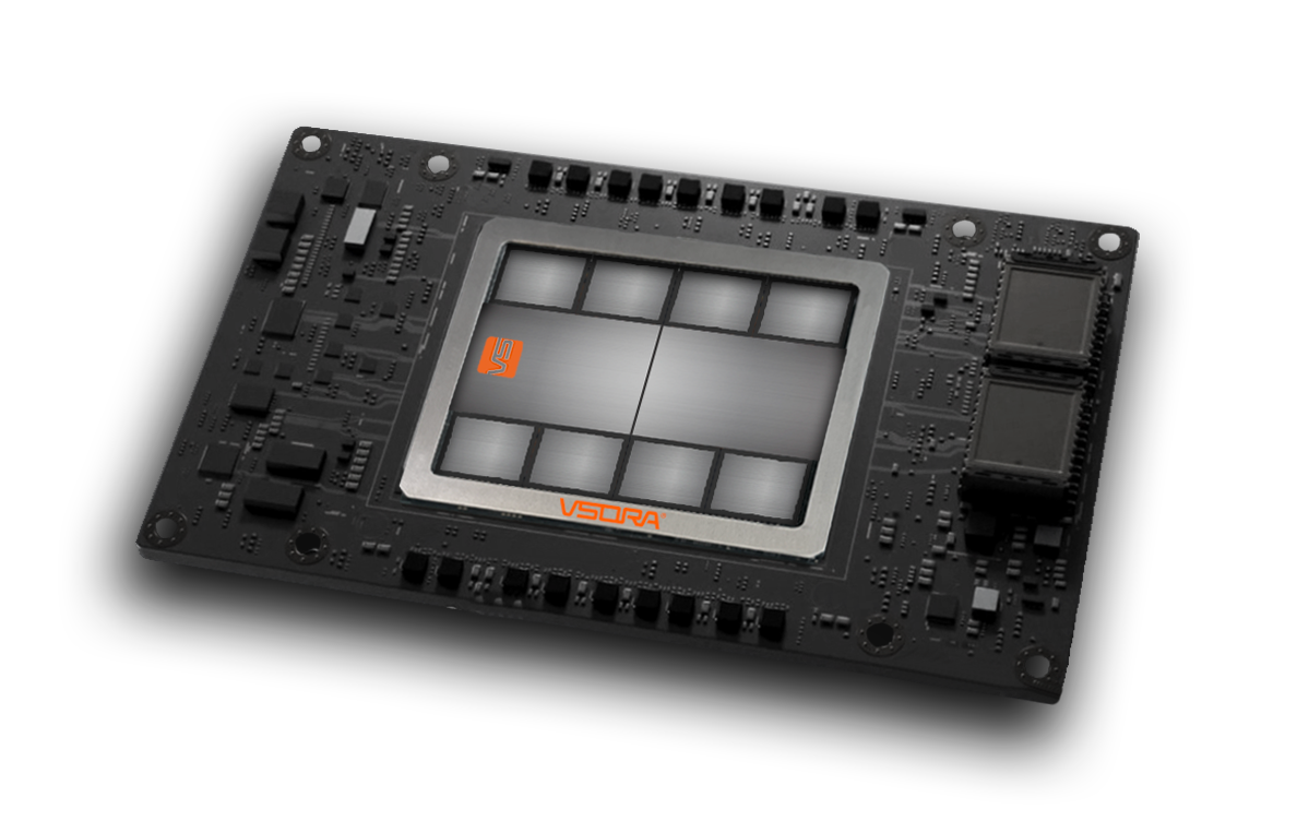
- VSORA’s new architecture achieves near-theoretical AI inference performance by eliminating the “memory wall” with a unified SRAM array.
- Each core features 16 million registers and high-throughput MAC units, supporting flexible tensor operations and dynamic precision.
- Chiplet-based scalability enables configurations for both datacenter (Jotunn8) and edge AI, offering significant power efficiency gains.
Charts
Understanding and Mitigating Column-Based Read Disturbance in DRAM Chips
Researchers at ETH Zurich and CISPA have identified and characterized a new widespread read disturbance phenomenon called “ColumnDisturb” in commodity DRAM chips. Unlike previous disturbances, ColumnDisturb can affect cells across multiple DRAM subarrays by repeatedly opening or keeping an aggressor row open, inducing bitflips in cells sharing the same columns. Experimental results from 216 DDR4 and 4 HBM2 chips show that this issue affects all major manufacturers and worsens as DRAM technology scales down, with the minimum time to induce a bitflip reducing by up to 5.06x. This trend suggests ColumnDisturb will pose significant challenges for future DRAM chips, impacting refresh mechanisms and data reliability.

- A new “ColumnDisturb” read disturbance affects DRAM cells across multiple subarrays, causing bitflips.
- This phenomenon worsens with DRAM technology scaling, reducing the time to induce bitflips by up to 5.06x.
- ColumnDisturb poses significant reliability challenges for future DRAM designs and refresh mechanisms.
Research
Utilizing Chiplet-Locality For Efficient Memory Mapping In MCM GPUs (ETRI, Sungkyunkwan Univ.)
Researchers from ETRI and Sungkyunkwan University have introduced CLAP (Chiplet-Locality Aware Paging), a novel approach to enhance memory mapping efficiency in Multi-Chip Module (MCM) GPUs. MCM designs introduce memory system non-uniformity when threads access remote chiplet resources, which is sensitive to page size. CLAP addresses this by determining the optimal page size for each application, leveraging the observation that GPU applications exhibit “chiplet-locality”—specific groups of pages primarily accessed by the same chiplet. By pre-organizing these local page groups into contiguous physical frames within the accessing chiplet, CLAP creates regions that function like large pages with merged TLB entries, delivering up to a 19.2% performance improvement over previous paging schemes.

- CLAP optimizes memory mapping in MCM GPUs by identifying and exploiting “chiplet-locality.”
- It dynamically determines suitable page sizes for applications, consolidating local page groups for efficient access.
- This approach improves performance by up to 19.2% by delivering the benefits of large pages without compromising locality.
Insight
Like Simulation Acceleration on GPUs. Innovation in Verification
A new paper titled “GEM: GPU-Accelerated Emulator-Inspired RTL Simulation” by Peking University and NVIDIA introduces a novel method to accelerate logic simulation on GPUs, addressing previous challenges with GPU architectures. Paul Cunningham (GM, Verification at Cadence) highlights Cadence’s continued investment in this area, noting that GEM’s intelligent partitioning and bit-packed structure enable efficient execution on NVIDIA’s SIMT machines. Raúl Camposano (Silicon Catalyst, former Synopsys CTO) praises GEM’s innovations, particularly its “boomerang executor layer” for intra-block efficiency and multi-stage RepCut partitioning for scalability, achieving up to 9x speed-up over leading commercial simulators. While currently lacking features like 4-state logic and multi-GPU support, GEM’s open-source, software-only approach represents a significant step forward in verification efficiency.

- GEM utilizes a new GPU-accelerated approach for RTL simulation, inspired by FPGA emulators.
- It achieves up to 9x speed-up over commercial simulators by optimizing logic execution for GPU architectures.
- Industry leaders recognize its potential for verification efficiency, despite current limitations in full commercial feature parity.
Stay connected with us for the most pivotal advancements shaping the future of the semiconductor landscape!