
News
Kerala Positions Design and IP at Core of Chip Strategy
The Indian state of Kerala has unveiled its Vision 2031 framework, charting a design-first semiconductor roadmap. Instead of investing heavily in multi-billion-dollar fabs, the state aims to focus on chip design, testing, and IP creation. This strategy leverages Kerala’s strong academic base to build design-centric clusters, expand hardware incubation centers, and retain intellectual property within India. The plan seeks to create half a million IT jobs and grow the sector’s economic output to $49.7 billion by 2031.

- Kerala prioritizes chip design, testing, and IP creation over fab construction.
- The strategy aims to create 500,000 IT jobs and boost economic output by 2031.
- Leverages academic strengths to build design-centric clusters and retain IP in India.
Launches
Qualcomm Snapdragon 8 Gen 4 Unveiling is Expected on October 24
Qualcomm is set to unveil its next-generation flagship mobile platform, the Snapdragon 8 Gen 4, on October 24. This highly anticipated chip is expected to power premium Android smartphones in 2025, bringing significant advancements in performance, AI capabilities, and power efficiency. The launch event is slated to showcase Qualcomm’s latest innovations in mobile processing, aiming to set new benchmarks for the industry and enhance user experiences across various high-end devices.

- Qualcomm to unveil its Snapdragon 8 Gen 4 mobile platform on October 24.
- The new chip is expected to deliver significant performance and AI enhancements.
- Aims to power premium Android smartphones in 2025, setting new industry benchmarks.
Charts
Overcoming BEOL Patterning Challenges at the 3-NM Node
At the 3-nm node, achieving precise interconnect critical dimensions (CD) and pitch for metal dimensions below 18 nm poses significant challenges, particularly in controlling Edge Placement Error (EPE). Through virtual fabrication and Monte Carlo simulations using SEMulator3D®, Lam Research identified critical process parameters and optimal process windows needed to manage EPE variability and line CD control. The analysis showed that only a small percentage of simulated runs met minimum line CD criteria, highlighting the importance of tightly controlling process parameters for successful patterning in advanced BEOL technologies.

- BEOL patterning at 3nm faces critical challenges with interconnect CD and EPE.
- Virtual fabrication identified key process parameters and windows for EPE control.
- Only 9.75% of simulated runs met line CD success criteria, emphasizing strict process control.
Research
P-type Layer Etch for Enhanced Deep UV LEDs to Boost Efficiency
Researchers in China have demonstrated an innovative method to enhance the performance of aluminium gallium nitride (AlGaN) deep ultraviolet (DUV) light-emitting diodes (LEDs) by carefully etching away DUV-absorbing p-type layers. This technique aims to increase light-extraction efficiency (LEE) without significantly compromising internal quantum efficiency (IQE) or carrier injection. The team found that an optimal etch depth can lead to improved light output power and wall-plug efficiency, crucial for developing more efficient DUV sources for sterilization and medical applications.
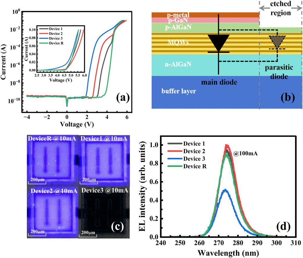
- P-type layer etching enhances DUV-LED light extraction efficiency.
- Balancing etch depth is crucial to prevent IQE reduction and increased resistance.
- Optimal etching shows improved light output power and wall-plug efficiency.
Insight
TEL to Highlight Sustainability Through Digitization and AI at SEMICON Europa 2025
At SEMICON Europa 2025, Tokyo Electron (TEL) will present on “Enabling Sustainability through Digitization and AI.” Kaushik Kumar will discuss how the semiconductor market, projected to reach $1 trillion by 2030 driven by AI, faces increasing complexities in device structures. The presentation will explore how semiconductor production equipment makers like TEL can leverage AI to manage these challenges sustainably, improve operational efficiency, and support Net-Zero objectives amidst rising development costs and extended timelines.

- TEL to present on sustainability, digitization, and AI at SEMICON Europa 2025.
- Focuses on leveraging AI to manage complexities and enhance efficiency in chip manufacturing.
- Aims to support Net-Zero objectives in the semiconductor industry’s growth towards $1 trillion by 2030.
Stay tuned for more essential updates and analysis shaping the future of the semiconductor industry!