
News
Intel Enters Lucrative ASIC Business, Forms Central Engineering Group
Intel is strategically entering the custom Application-Specific Integrated Circuit (ASIC) market, historically dominated by companies like Broadcom and Marvell. This move involves establishing a new Central Engineering Group to enhance engineering execution, leverage Intel’s x86 IP, and offer design services to external customers. The global ASIC market, valued at over $20 billion in 2025, is projected to double in five years due to demand from AI, edge computing, and 5G/6G. Intel’s approach is to offer custom ASICs centered around Intel/NVIDIA IP using Intel Foundry manufacturing and packaging.
- Intel forms a Central Engineering Group to spearhead a new ASIC and design services business.
- Aims to leverage core x86 IP and Intel Foundry capabilities for purpose-built silicon.
- Targets the rapidly growing $20B+ ASIC market, driven by AI and edge computing demand.

Launches
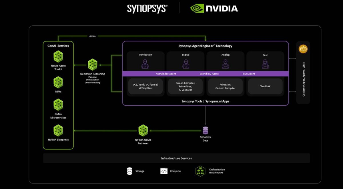
Synopsys and NVIDIA Deepen Partnership for AI-Powered Chip Design
Synopsys and NVIDIA are expanding their three-decade collaboration, integrating Synopsys’ software with NVIDIA’s agentic AI, GPU-accelerated computing, and AI-driven physics simulations. This partnership aims to revolutionize semiconductor design by transforming AI into a collaborative design partner. Key initiatives include fusing Synopsys’ AgentEngineer™ with NVIDIA’s NeMo Agent Toolkit for autonomous design flows and leveraging NVIDIA GPUs for up to 500x speedup in fluid simulations and 15x gains in atomistic simulations. This targets faster iterations, reduced energy consumption, and scalable simulations for advanced nodes and complex systems.
- Partnership integrates Synopsys’ tools with NVIDIA’s agentic AI, GPU-accelerated computing, and AI physics.
- Aims to transform AI into a collaborative partner for autonomous design flows, enhancing productivity.
- Promises significant performance speedups (e.g., 500x in fluid simulations) across EDA and simulation workloads.
Charts
The High Cost of Verification: AI’s Untapped Potential
Industry analysis consistently shows that over 50% of IC/ASIC project time is dedicated to verification, requiring as many verification engineers as design engineers. Debugging alone accounts for a substantial 47% of this verification effort, making it a prime area for efficiency improvements. While AI-generated RTL currently sees an acceptance rate of only around 25%, indicating limitations in reliability and complexity, agentic AI approaches hold significant promise for enhancing verification processes, particularly in bug triage and root-cause analysis, where substantial ROI can be realized.
- Over 50% of IC/ASIC project time is spent on verification, matching design time.
- Debugging consumes 47% of all verification effort, presenting a major efficiency challenge.
- Agentic AI offers significant ROI potential in bug triage and root-cause analysis for verification.

Research
Penn State and NIWC Develop Three-Terminal Memtransistors for Edge AI
Researchers from Penn State University and Naval Information Warfare Center Pacific have developed large-scale crossbar arrays based on three-terminal MoS2 memtransistors. These novel devices are designed for efficient, low-power inference engines in edge AI applications. Unlike traditional memristive crossbars, these memtransistors can dynamically tune conductance via gate control, effectively resolving similar outputs and enhancing separability without retraining. The technology demonstrates high yield (>92%), low write energies (~0.2 fJ), and projected retention exceeding three years, validating performance with MNIST digit classification.
- New MoS2 memtransistors offer dynamic conductance tuning via gate control for enhanced inference.
- Achieve high yield (>92%), low write energies (~0.2 fJ), and long retention (>3 years).
- Aims to improve separability in edge AI applications without costly retraining.

Insight
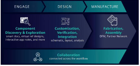
Redefining OEM Component Discovery with Interactive Digital Tools
The semiconductor industry is seeing a shift in how component manufacturers engage with OEM hardware designers. A new approach emphasizes interactive digital tools and AI-powered chatbots to streamline component discovery, replacing cumbersome datasheet reviews. Manufacturers are offering interactive reference designs, allowing designers to experiment with parameters and view impacts on behavior directly. This “engineering outreach” provides access to schematics, PCB layouts, and BOMs, alongside supply chain and compliance information, fostering early design commitment and manufacturer stickiness before traditional sales engagement.
- New models use interactive tools and AI to simplify component discovery for OEMs.
- Designers can experiment with virtual reference designs, schematics, and BOMs.
- Aims to foster early design wins and manufacturer loyalty through enhanced digital engagement.
Stay connected with us for the latest developments shaping the future of the semiconductor industry.