
TSMC Arizona N4 Production Begins
TSMC Arizona Begins N4 Production, Boosting Domestic Chip Manufacturing
TSMC’s highly anticipated N4 process technology has officially begun volume production at its first fabrication plant in Arizona, marking a significant milestone for domestic semiconductor manufacturing in the United States. This move is expected to bolster the U.S. supply chain for advanced chips, with initial production focused on customers like Apple and Nvidia. The ramp-up of this facility underscores the strategic importance of localized, leading-edge chip production.

- First U.S.-based fab to initiate volume production of N4 process technology.
- Aims to strengthen the domestic semiconductor supply chain and reduce reliance on overseas manufacturing.
- Expected to serve major customers requiring advanced chip designs.
Eta Compute Rebrands as ModelCat, Unveils Agentic Model Builder
ModelCat Launches Agentic AI Platform for Hardware-Aware Edge AI Model Building
Eta Compute, an AI software startup, has rebranded as ModelCat and introduced an innovative agentic AI platform designed for hardware-aware model building on edge devices. This new platform uses an AI agent to automate the complex process of creating tailored models, significantly reducing manual effort and optimizing performance for specific edge hardware constraints. The tool tests hypotheses on real hardware in the cloud, delivering models optimized for metrics like latency, energy consumption, and prediction accuracy.

- Automates edge AI model creation using an AI agent, accelerating development.
- Optimizes models for specific hardware constraints, including latency and energy efficiency.
- Partnership with NXP integrates a dedicated version into the eIQ software ecosystem.
Gartner Forecasts Global Semiconductor Revenue to Grow 18 Percent in 2025
Gartner Projects Robust 18% Growth in Global Semiconductor Revenue for 2025
Market research firm Gartner forecasts an impressive 18% increase in global semiconductor revenue for 2025, reaching a projected $706 billion. This significant growth is primarily driven by the escalating demand for chips in AI applications, particularly for generative AI inference and training. Memory segment recovery, especially DRAM, is also a key factor contributing to this optimistic outlook, as the market rebounds from previous downturns. The forecast underscores the pivotal role of advanced computing and memory in driving overall industry expansion.

- Global semiconductor revenue expected to hit $706 billion in 2025.
- AI applications, including generative AI, are identified as major growth accelerators.
- Memory market recovery, led by DRAM, significantly contributes to the forecasted expansion.
Silicon Photonic Interconnected Chiplets With Computational Network And IMC For LLM Inference Acceleration (NUS)
NUS Introduces PICNIC: Photonic Interconnected Chiplets for LLM Inference
Researchers at the National University of Singapore (NUS) have published a technical paper detailing “PICNIC,” a 3D-stacked chiplet-based accelerator designed to significantly improve Large Language Model (LLM) inference performance. PICNIC integrates non-volatile in-memory computing (IMC) processing elements and an Inter-PE Computational Network, all interconnected via silicon photonics to address critical communication bottlenecks. Simulations show impressive results, with up to 57x efficiency improvement over Nvidia H100 in accommodating larger models.
- Utilizes 3D-stacked chiplets with silicon photonic interconnects to overcome communication bottlenecks.
- Integrates in-memory computing (IMC) for enhanced processing efficiency.
- Achieves substantial speedup and efficiency gains for large language model inference.
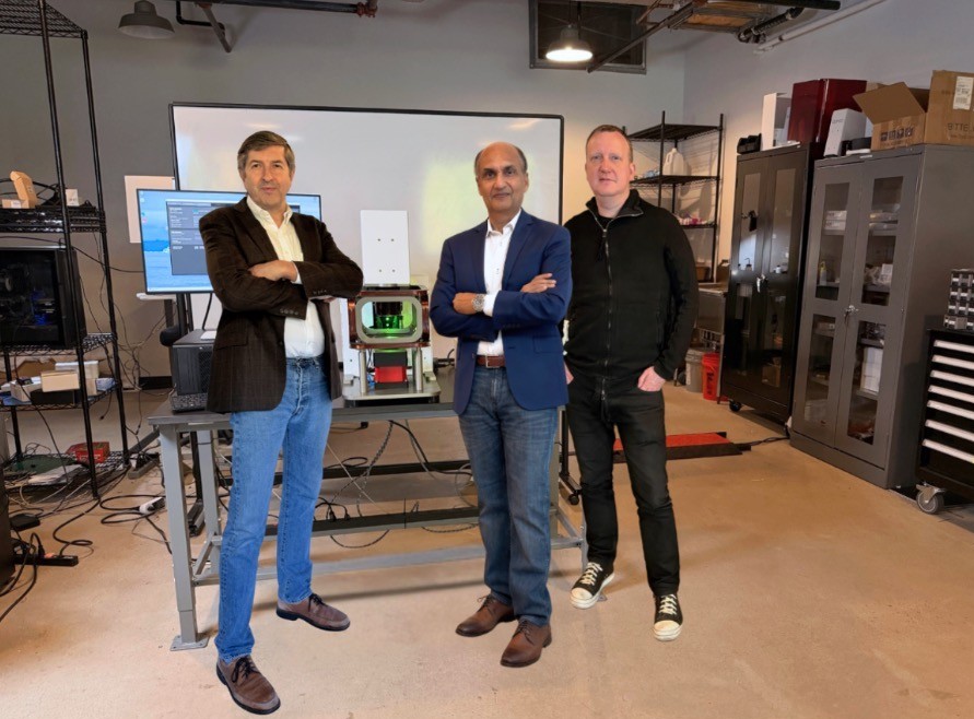
CEO Interview with Sanjive Agarwala of EuQlid Inc.
EuQlid CEO Details Quantum 3D Imaging for Advanced Semiconductor Metrology
Sanjive Agarwala, co-founder and CEO of EuQlid, shared insights into the company’s proprietary quantum 3D imaging platform, Qu-MRI™. This technology provides non-destructive, high-precision mapping of buried current flow, addressing a critical unmet need in metrology for advanced semiconductor (3D heterogeneous integration) and battery design and manufacturing. EuQlid aims to fill the whitespace in inspecting buried interconnects for defects that current tools cannot reach, ensuring quality and optimizing complex manufacturing workflows.
- Qu-MRI™ platform offers non-destructive 3D imaging of sub-surface current flow.
- Addresses critical metrology gaps in advanced semiconductor and battery manufacturing.
- Enables precise inspection of buried device structures and interconnect integrity.
Stay tuned for more cutting-edge developments and insights shaping the semiconductor industry’s future.