News
Arm’s DreamBig Acquisition Reignites In-House Chip Prospects
Arm has acquired DreamBig Semiconductor for $265 million, signaling a strategic move to capitalize on the surging AI and data center demand. DreamBig, known for its Chiplet Hub technology and Mercury AI-SuperNIC, could help Arm expand beyond its traditional IP licensing model. This acquisition fuels speculation that Arm might begin developing and selling its own chips, especially in the AI networking and data center sectors.

- Arm’s acquisition targets DreamBig’s chiplet and AI networking solutions.
- The move suggests Arm may explore selling its own chips, not just IP, for AI data centers.
- This strategic shift could intensify competition with existing Arm licensees in the AI silicon market.
Launches
Ceva Unleashes Wi-Fi 7 Pulse Awakening Instant AI Brains in IoT
Ceva has launched the Ceva-Waves Wi-Fi 7 1x1 client IP, designed to power AI-enabled IoT devices and physical AI systems with unprecedented responsiveness. Leveraging the IEEE 802.11be standard, this IP core delivers ultra-high performance in compact, power-constrained form factors, essential for the projected 30 billion IoT devices by 2030. It integrates seamlessly with Ceva’s NeuPro NPUs, enabling on-device intelligence and reducing reliance on cloud processing.

- The Wi-Fi 7 IP enhances AI-enabled IoT with low-latency, high-throughput connectivity.
- Features like Multi-Link Operation and 4096-QAM boost performance for real-time applications.
- Integration with NPUs facilitates on-device AI processing, improving data privacy and battery life.
Charts
AI Chip Market Size Projected for Significant Growth Through 2030
The global AI chip market is experiencing explosive growth, driven by increasing adoption across diverse sectors from data centers to edge devices. Industry reports indicate a substantial upward trajectory in market size, with forecasts predicting continued expansion at a robust compound annual growth rate through 2030. This growth underscores the foundational role of specialized AI silicon in advancing artificial intelligence capabilities.

- The AI chip market is forecasted for rapid expansion, propelled by demand for AI processing.
- Growth is evident across various applications, from cloud AI to edge intelligence.
- Specialized AI hardware is critical for enabling next-generation AI models and services.
Research
3D Guard-Layer: An Integrated Agentic AI Safety System for Edge AI
Researchers from Princeton, HKUST, and NC State University have published a technical paper introducing “3D Guard-Layer,” an integrated agentic AI safety architecture for Edge AI. This novel system leverages 3D integration to embed a dedicated safety layer directly within edge devices. It’s designed to dynamically learn and mitigate attacks against AI systems, enhancing resilience, reliability, and performance with minimal overhead for edge computing hardware.

- Proposes a 3D integrated safety layer for Edge AI to combat security vulnerabilities.
- The system offers adaptive learning capabilities to mitigate evolving AI attacks.
- Enhances resilience, reliability, and modularity for AI deployment at the edge.
Insight
Hierarchically Defining Bump and Pin Regions Overcomes 3D IC Complexity
Experts from Siemens EDA emphasize the critical role of hierarchical device planning in managing the explosive complexity of modern IC packaging, especially with 3D ICs and chiplet integration. With pin counts surging into the millions, traditional “flat” design methodologies are no longer sufficient. Hierarchical planning provides an abstraction layer, enabling designers to optimize functional areas, conduct early multi-domain analyses (SI, PI, thermal), and significantly reduce costly redesigns.
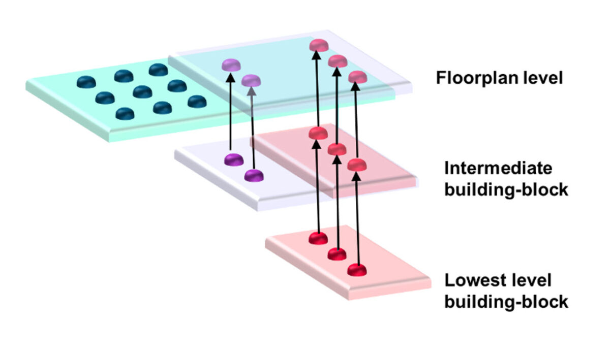
- Hierarchical device planning is crucial for managing the immense complexity of 3D IC and chiplet packaging.
- It allows abstraction of millions of pins into manageable regions, enhancing design efficiency.
- Early multi-domain analysis is vital for informed design decisions and preventing expensive re-spins.
Stay connected with us for the latest breakthroughs and developments shaping the semiconductor landscape!