
News
China Photoresist Maker Hengkun Goes Public on STAR Market with YMTC-Tied Fund
Xiamen Hengkun New Material, a prominent Chinese photoresist manufacturer, has successfully debuted on the Shanghai STAR Market, securing RMB 1.01 billion. This significant funding is earmarked for expanding its IC precursor and advanced IC materials projects, underscoring China’s strategic drive to bolster domestic capabilities in critical semiconductor materials and reduce reliance on imports.
- Hengkun’s product portfolio, including SOC, BARC, KrF, and i-Line photoresists, are in mass production, supporting advanced 3D NAND, DRAM, and sub-14nm logic chips.
- The IPO capital will substantially boost the production of KrF/ArF photoresists and precursor materials.
- The company’s impressive growth in KrF photoresists and successful validation of ArF immersion photoresists signify accelerating domestic substitution trends.
Launches
Aniah Revolutionizes Electrical Verification in IC Design with OneCheck®
Aniah has introduced OneCheck®, a pioneering static transistor-level Electrical Rule Checking (ERC) tool, poised to tackle the pervasive bottleneck in IC design verification. With industry reports indicating that 86% of IC/ASIC designs necessitate respins due to flaws, OneCheck® aims to enable “right-on-first-silicon” by automating verification processes, drastically minimizing false positives, and providing unparalleled error coverage across increasingly complex designs.
- OneCheck® performs full-chip analysis across all possible power combinations, rigorously detecting errors like conditional HiZ, missing level shifters, and electrical overstress.
- It integrates seamlessly with Cadence Virtuoso, allowing for early-stage implementation and processing of billion-transistor designs within minutes.
- The tool significantly enhances debugging efficiency and overall productivity by identifying and grouping root causes of errors.
Charts
Ultra-broadband Wide-angle Anti-reflection Scheme Utilizing Multi-layer Resonant Metasurfaces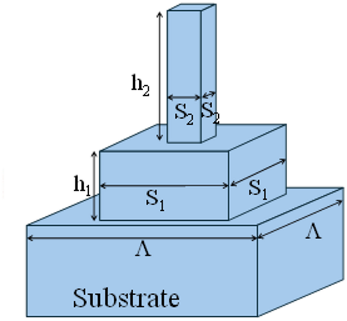
A novel hybrid anti-reflection (AR) scheme employing multi-layer resonant metasurfaces has been developed, showcasing ultra-broadband and wide-angle performance. Demonstrated for Silicon-Air interfaces in the telecom band, this monolithic, single-material design exhibits remarkable robustness against fabrication errors and is ideally suited for high-power applications, offering a significant improvement over conventional thin-film coatings.
- The scheme precisely optimizes meta-atom dimensions to tailor metasurface resonances, achieving reflection suppression beyond -30dB across the 1300-1700 nm wavelength range and for incidence angles up to ±30°.
- Design robustness was confirmed through analysis showing minimal impact from typical fabrication dimension variations (e.g., ±5-10 nm for meta-atoms, ±10-20 nm for thickness).
- This approach is compatible with additive manufacturing techniques, including 3D printing and Nano-Imprint Lithography, facilitating scalable production for diverse optical systems.
Research
Blend Strategy To Improve Edge Resistance Capability And Thickness Of EUV-Fabricated Nanopatterns
Researchers at National Tsing Hua University have unveiled a groundbreaking blend strategy for tin-oxide (SnO) photoresists, significantly enhancing both the edge resistance and thickness of EUV-fabricated nanopatterns. By combining two distinct tin oxide carboxylate clusters, the resulting photoresist achieved exceptional EUV resolutions (13-16 nm half-pitch) at notably low exposure doses (50-60 mJ/cm²), alongside marked improvements in etching resistance.
- This blend strategy leverages one 12-oxide cluster to specifically boost pattern resolution, etching resistance, and nanopattern thickness, while photosensitivity is primarily driven by the other cluster.
- The innovation directly addresses persistent challenges of limited thickness and poor etching resistance commonly encountered in current metal carboxylate cluster EUV photoresists.
- Cooperative interactions between the clusters yielded an outstanding Z-factor (2.65 × 10⁻⁸ mJ·nm³), indicative of superior overall lithographic performance.
Insight
Global Semiconductor Outlook 2025: Key Trends and Forecasts by Industry Leaders
Leading figures in the semiconductor industry recently shared their projections for 2025, emphasizing the sustained and accelerating growth of Artificial Intelligence (AI) and High-Performance Computing (HPC) as pivotal drivers of semiconductor demand. Despite anticipated macroeconomic variability, executives highlighted the imperative of strategic investments in advanced manufacturing, comprehensive R&D, and robust supply chain resilience. A key focus is the industry’s ongoing shift towards specialized architectures and heterogeneous integration to effectively meet evolving demands for performance and power efficiency.
- AI and HPC are forecast to be the primary engines for significant growth, necessitating continued advancements in packaging and process technologies.
- Ongoing efforts in supply chain diversification and regionalization aim to mitigate geopolitical risks and enhance overall resilience.
- The industry is placing a heightened focus on sustainability and energy efficiency, integrating these principles into both chip design and manufacturing processes.
Stay connected with us for the latest news and breakthroughs shaping the semiconductor landscape!