
News
Ainekko Buys Esperanto Hardware IP, Open-Sources It
Open-source AI hardware and software startup Ainekko has acquired the IP and selected assets of AI chip startup Esperanto Technologies, including its chip designs, software tooling, and development framework. Ainekko plans to open-source Esperanto’s production-grade many-core RISC-V architecture, including RTL, reference designs, and development tools, with the goal of fostering community innovation and focusing on power-efficient edge AI applications.

- Ainekko acquires Esperanto’s RISC-V AI chip IP, making it open-source.
- Aims to drive innovation for edge AI, robotics, and embedded devices.
- Plans include a TSMC tapeout and future ASIC design services leveraging the open architecture.
Launches
Self-terminating recess etch produces nitride transistor with +3V threshold
Researchers from Peking and Xidian universities have developed a self-terminating gate recess etch process that enables the production of aluminium gallium nitride (AlGaN) normally-off metal-oxide-semiconductor field-effect transistors (MOSFETs) with positive threshold voltages of up to +3.2V. This advancement is critical for high-frequency and high-power applications, leading to more reliable and energy-efficient devices by ensuring fail-safe operation.
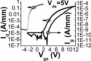
- New self-terminating gate recess etch process for AlGaN MOSFETs.
- Achieves a high positive threshold voltage of +3.2V for reliable normally-off operation.
- Enhances performance and power efficiency in high-frequency and high-power applications.
Charts
Minimizing Voltage Loss and Boosting Yield in Advanced GAA Transistors
A virtual study by Lam Research’s Semiverse Solutions team analyzed Gate-All-Around (GAA) devices using Backside Power Delivery Networks (BSPDN), comparing Direct Backside Contact (DBC) and Self-Aligned Backside Contact (SABC) architectures. The study, which includes process window contour diagrams, demonstrates that SABC significantly minimizes edge placement error (EPE) and over-etch variations, providing a much larger and more stable process window than DBC, thus promising higher yield for advanced logic nodes.

(Refer to the original article for “Figure 2. Comparison of SABC and DBC process windows”)
- Virtual study compares SABC and DBC architectures for advanced GAA transistors with BSPDN.
- SABC approach offers a significantly larger and more stable process window.
- Minimizes EPE and over-etch variations, leading to higher yield for future logic device scaling.
Research
Crypto Mining ASIC Goes Deep Sub-Threshold on 3 nm
Japanese company Triple-1 is taping out its Kamikaze III Bitcoin-mining ASIC on TSMC’s 3nm process, boasting a power efficiency of 10.45 J/TH through proprietary sub-threshold design techniques. This groundbreaking approach, requiring custom cell design and manual routing, not only pushes the boundaries of power efficiency for crypto mining but also positions the company to develop future AI accelerator chips optimized for edge applications, leveraging its expertise in power management and distributed computing.

- Triple-1’s Kamikaze III ASIC on TSMC 3nm achieves extreme power efficiency with proprietary sub-threshold design.
- Highlights innovative custom cell design and manual routing for ultra-low voltage operation.
- Explores a transition to AI accelerator chips for edge computing and distributed energy solutions.
Insight
D-Wave Among Few Ramping Quantum Computer Sales
D-Wave’s Chief Development Officer Trevor Lanting discussed the company’s increasing sales of quantum annealing systems, including a significant installation at the Jülich Supercomputing Center for integration with Europe’s Jupiter exascale computer. Lanting provided key insights into D-Wave’s strategic pivot towards developing more challenging gate-model quantum technology, driven by critical innovations in error correction methodologies and fundamental qubit design, emphasizing the long-term vision for quantum applications.

- D-Wave reports growing sales of its quantum annealing systems, including deployments for exascale supercomputer integration.
- Outlines a strategic pivot to gate-model quantum technology, citing advancements in error correction and qubit design.
- Leverages existing foundry partnerships for the development of both annealing and gate-based quantum processors.
Stay connected with us for the latest news and breakthroughs shaping the semiconductor landscape.