
News
Ainekko Buys Esperanto Hardware IP, Open-Sources It
Ainekko, an open-source AI hardware and software startup, has acquired the IP and select assets of AI chip startup Esperanto Technologies. This includes chip designs, software tooling, and development framework, which Ainekko plans to open-source.

- Ainekko will open-source Esperanto’s production-grade many-core RISC-V architecture for increased flexibility and community engagement.
- The initiative targets edge AI applications where power efficiency is critical, rather than hyperscale data centers.
- Ainekko plans its first silicon tapeout with eight Esperanto cores and MRAM, aiming for an intermediate 256-core design next.
Launches
Imec.kelis: tool for AI datacenter design and optimization
Imec has launched imec.kelis, an analytical performance modeling tool designed to optimize the design of AI datacenters. This cutting-edge tool provides a fast, transparent, and validated framework for evaluating system performance across compute, communication, and memory subsystems, specifically tailored for large language model (LLM) training and inference workloads.

- Imec.kelis offers an end-to-end framework for AI datacenter design, enabling architects to balance performance, sustainability, and cost.
- It leverages imec’s expertise in system-level modeling and hardware-software co-design, with predictions validated on industry-standard platforms.
- Key features include an LLM task-graph analyzer, a hierarchical roofline model, and an interactive dashboard for design space exploration, validated within a 12% error margin.
Charts
Semiconductors Up Over 20% in 2025
The world semiconductor market reached a record $208 billion in Q3 2025, marking the first time it surpassed $200 billion. This represents a 15.8% increase from Q2 2025 and a 25.1% rise from Q3 2024, driven significantly by AI demand. Nvidia remained the top supplier with $57.0 billion in revenue.
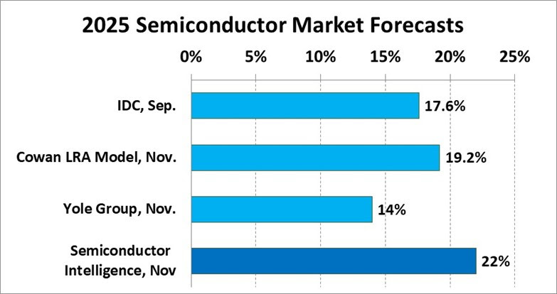
- The semiconductor market achieved a record $208 billion in Q3 2025, reflecting robust growth of over 20% year-over-year.
- AI-driven demand, particularly for memory and AI accelerators, is identified as the primary catalyst for this strong market performance.
- The market is projected to continue growing by 12% to 18% in 2026, with potential moderation in AI-dependent sectors and stronger growth in other segments like PCs and smartphones.
Research
Quantum Sensor Startup Seeks Flaws in 3D Chips
EuQlid, a quantum technology startup, is developing a novel quantum sensor platform called QuMRI to non-destructively detect buried defects in 3D chips. This technology, based on artificial diamonds with nitrogen-vacancy (NV) centers, aims to quickly map current flows in deeply buried interconnects, potentially saving billions of dollars in manufacturing.

- QuMRI uses quantum sensors from artificial diamonds to precisely map current flows and detect defects in 3D stacked chips without damage.
- The technology is significantly faster (100x) than X-ray inspection and offers similar precision to depths required by the semiconductor industry.
- This innovation addresses critical challenges in 3D chip manufacturing by providing a non-destructive method for quality control, improving yield and reducing costs.
Insight
The Future For Formal Verification
An expert panel discussed the evolving role of formal verification (FV) in the semiconductor industry, particularly with the advent of Agentic AI. The conversation highlighted FV’s potential to move beyond traditional functional verification, playing a crucial role in validating AI-generated designs, identifying unknown unknowns, and addressing challenges in security, functional safety, power, and thermal analysis.

- Agentic AI is expected to transform EDA by generating design code and assertions, with formal verification essential for ensuring correctness and completeness.
- Experts believe the industry is shifting towards natural language specifications, with LLMs assisting in translating these into machine-readable formats and SVA properties.
- Beyond functional verification, FV is being applied to critical areas like security, power optimization (e.g., clock gating), functional safety (FuSa), and identifying worst-case performance scenarios.
Stay tuned for more essential updates as the semiconductor landscape continues to evolve with groundbreaking advancements and market shifts.