News
Accelerated EDA Development Addresses Plummeting First-Silicon Success Rates
First-silicon success rates have dropped to a historic low of 14%, posing a significant challenge to the semiconductor industry, particularly as it advances towards 2nm process nodes. Traditional on-premises infrastructure struggles to meet the compute and memory demands for advanced verification workflows.
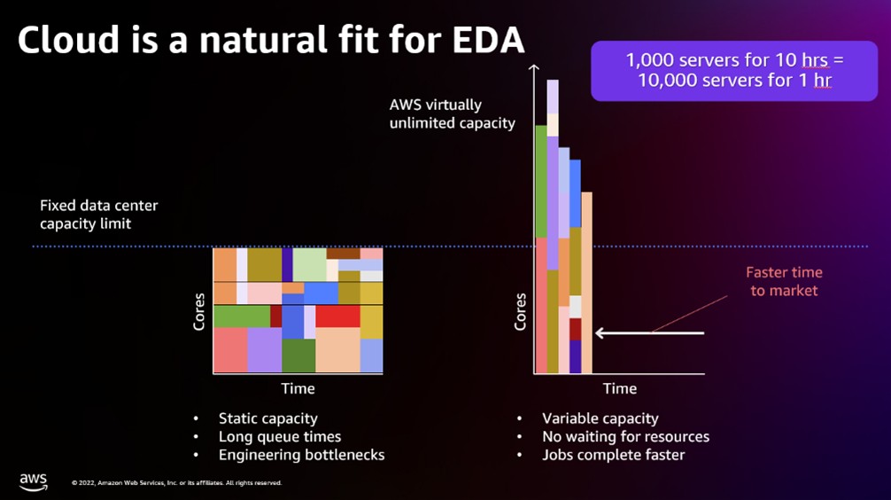
- Cloud environments, through partnerships like AWS and NetApp, offer elastic scaling, advanced analytics, and robust security essential for next-generation verification.
- AI-driven optimization and real-time analytics enable data-driven decisions, reducing verification cycle times and improving efficiency.
- Embracing cloud transformation is critical for addressing verification complexities and enhancing silicon success rates in the 2nm era and beyond.
Launches
Heidelberg Instruments MLA 150 Maskless Aligner Celebrates 10 Years with Enhanced Capabilities
Heidelberg Instruments is marking a decade of innovation with its MLA 150 Maskless Aligner, a tool that has transformed high-resolution lithography in R&D and industry since 2015. Known for its flexibility, mask-free operation, and ease of use, the MLA 150 has become a staple in over 250 cleanrooms worldwide.
![]()
- The MLA 150 uses a digital micromirror device (DMD) for direct-write lithography, offering fast turnaround times and high accuracy.
- A significant upgrade in 2025 pushed the minimum feature size to 45 nm, expanding its utility for precision applications.
- It supports rapid innovation in quantum devices, MEMS, micro-optics, and biosensors, enabling users to go from design to patterned substrate in minutes.
Charts
Global Semiconductor Market Revenue Expected to Reach New Highs by 2030
The semiconductor industry is poised for robust growth in the coming years, with market revenue projected to continue its upward trajectory, potentially surpassing significant milestones by the end of the decade. This expansion is driven by increasing demand across various applications, including AI, automotive, and IoT, alongside advancements in manufacturing technologies.

- Market analyses indicate a strong rebound and sustained growth following recent fluctuations, reflecting underlying demand for advanced computing.
- Key drivers include the proliferation of AI accelerators, expansion of 5G infrastructure, and increasing adoption of smart technologies.
- Continued investments in R&D and manufacturing capacity are essential to support this projected market expansion.
Research
New Method Enhances Quantum Emitter Activation in SiC with Laser Annealing
Researchers have developed a novel approach for efficiently forming luminescent defects, specifically silicon vacancies (VSi−), in 4H-SiC using ion irradiation followed by nanosecond-pulsed laser annealing. These “color centers” are critical for developing single photon sources (SPS) for quantum technologies, offering potential room-temperature operation.
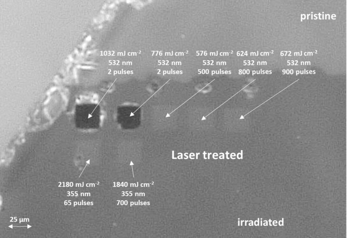
- The method allows for selective, localized activation of VSi− centers, significantly increasing activation yield compared to conventional thermal annealing.
- Laser pre-processing enables efficient activation of VSi− centers at lower subsequent thermal annealing temperatures, from 600 °C down to 300-450 °C.
- This technique is promising for scalable fabrication of robust quantum emitters in SiC for applications in quantum computing, cryptography, and sensing.
Insight
MIT Researchers Advance 3D Nanofabrication with Novel Directed Self-Assembly Method
MIT researchers have published a new technical paper detailing a hierarchical Directed Self-Assembly (DSA) method to create 3D interconnected networks in thin films. This breakthrough expands the utility of block copolymers (BCPs) beyond traditional 2D patterning, opening new avenues for nanoscale manufacturing.

- The method generates complex cross-point structures with connected in-plane and out-of-plane segments, offering controlled orientation.
- By combining surface modification, BCP periodicity, and topographic templates, highly ordered 3D networks like ladder and cross-point structures can be produced.
- This innovation significantly enhances BCP-derived nanofabrication capabilities, potentially impacting future device scaling and advanced material architectures.
Stay tuned for more essential updates as the semiconductor industry continues to innovate at an unprecedented pace.