- News: IC and Silicon Labs Raise the Bar for Hardware Security
- Launches: On-Package Memory With UCIe To Improve Bandwidth Density And Power Efficiency
- Charts: Why Choose PCIe 5.0 for Power, Performance and Bandwidth at the Edge
- Research: System-HW Co-Design Approach Combines Mono3D DRAM, NMP, and GPU Acceleration
- Insight: Heterogeneous System With Specialized HW For Disaggregated LLM Inference
Continue Reading →
- News: Arizona Benefits from TSMC, Intel, SEMICON West Debuts In Area
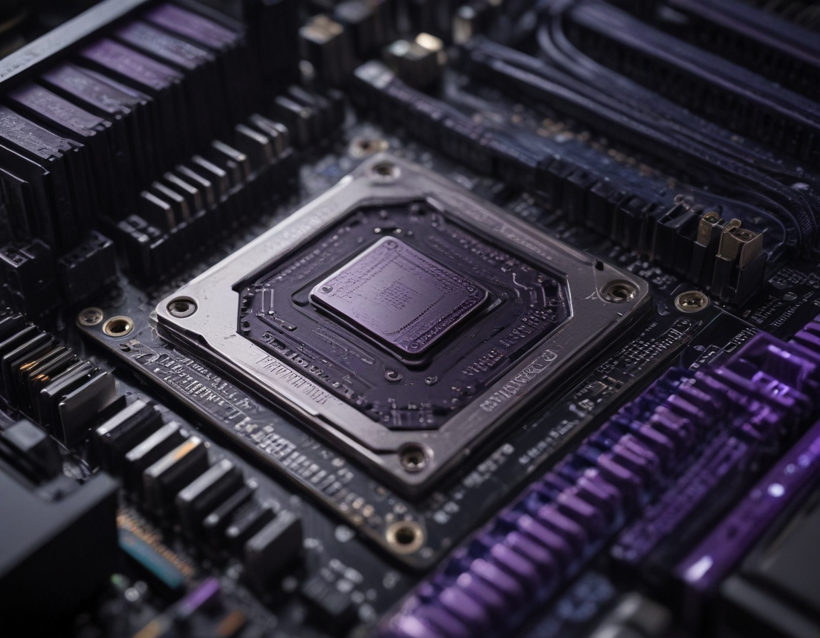
- Launches: Cinch Details CIN:APSE Interconnect Evolution for Harsh Environments
- Charts: The Future of Optoelectronic Devices for Medical Applications
- Research: AI-powered Method Helps Protect Global Chip Supply Chains from Cyber Threats
- Insight: CEO Interview with Gary Spittle of Sonical
Continue Reading →
- News: Lam Research Receives 2025 SEMI Award for North America
- Launches: Advanced Packaging Fuels Growth in the Semiconductor Back-End
- Charts: Global 300mm Fab Equipment Spending Expected to Total $374 Billion Over Next Three Years
- Research: Global Efficiency Record Set for Large, Triple-Junction Perovskite Solar Cell
- Insight: How 3D-IC Will Change Chip Design
Continue Reading →
- News: Double Duty Logic Block Architecture Enabling Concurrent LUT and Adder Chain Usage
- Launches: The path to smaller denser and faster
- Charts: AI Everywhere in the Chip Lifecycle: Synopsys at AI Infra Summit
- Research: In-SRAM Computing Architecture Tailored For Cryptographic Acceleration Within MCUs
- Insight: CEO Interview with Howard Pakosh of TekStart
Continue Reading →
- News: Qualcomm To Acquire Arduino
- Launches: ACM Research Unveils Ultra ECDP Electrochemical Deplating Tool for Compound Semiconductor Gold Etch Processes
- Charts: Volume Semiconductor Manufacturing Yield Improvement
- Research: Imec Achieves New Milestones in Single Patterning High NA EUV Lithography
- Insight: Emerson Leverages AI to Address Complexity in Test and Measurement
Continue Reading →
- News: ASML, Mistral AI enter strategic partnership
- Launches: NSR-S333F ArF Scanner Now Open for Orders
- Charts: Via Multipatterning Regardless of Wavelength
- Research: First Stage Of Nanoscale Imaging In Positive-Tone EUV Photoresists
- Insight: PLDC: A Robust MPC Solution for Any Mask Shape
Continue Reading →
See All ➡